OR4E10 ТЪЦуюІТЋИТЊџУАе№╝ѕPDF№╝Ѕ - Agere -> LSI Corporation
жЏХС╗Ху╝ќтЈи
С║ДтЊЂТЈЈУ┐░ (тіЪУЃй)
ућЪС║Дтјѓт«Х
OR4E10 Datasheet PDF : 124 Pages
| |||
Preliminary Data Sheet
December 2000
ORCA Series 4 FPGAs
Programmable Input/Output Cells (continued)
LVDS I/O
The LVDS differential pair I/O standard allows for high-speed, low-voltage swing and low-power interfaces defined
by industry standards: ANSI*/TIA/EIAРђа-644 and IEEE 1596.3 SSI-LVDS. The general-purpose standard is supplied
without the need for an input reference supply and uses a low switching voltage which translates to low ac power
dissipation.
The ORCA LVDS I/O provides an integrated 100 Рёд matching resistor used to provide a differential voltage across
the inputs of the receiver. The on-chip integration provides termination of the LVDS receiver without the need of dis-
crete external board resistors. The user has the programmable option to enable termination per receiver pair for
point-to-point applications or, in multipoint interfaces, limit the use of termination to bused pairs. If the user chooses
to terminate any differential receiver, a single LVDS_R pin is dedicated to connect a single 100 Рёд resistor to VSS,
which will provide a balance termination to all of the LVDS receiver pairs programmed to termination. See Table 20
for the LVDS termination pin location.
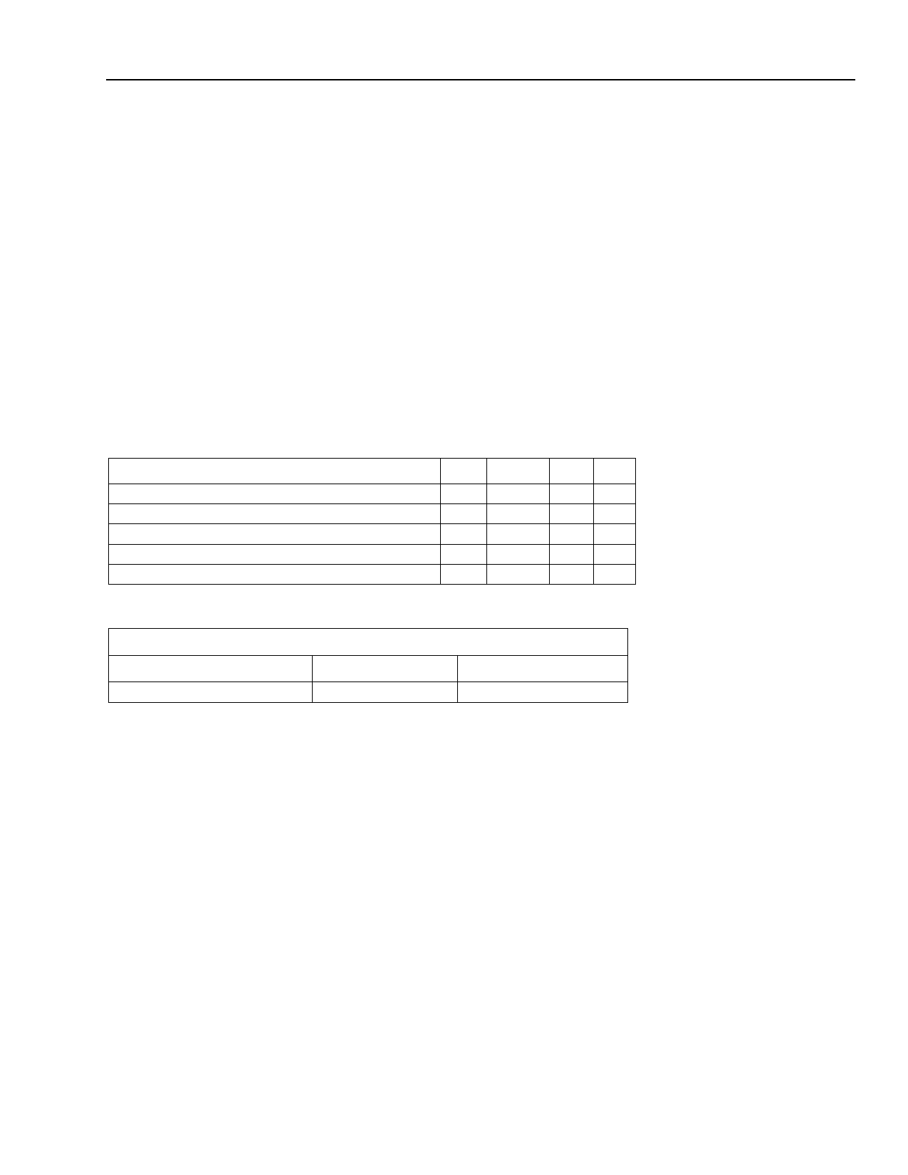
Table 19 provides the dc specifications for the ORCA LVDS solution.
Table 19. LVDS I/O Specifications
Parameter
Built-in Receiver Differential Input Resistor
Receiver Input Voltage
Differential Input Threshold
Output Common-mode Voltage
Input Common-mode Voltage
Min Typical Max Unit
95 100 105 Рёд
0.0
Рђћ
2.4 V
РђЊ100 Рђћ 100 mV
1.125 1.25 1.375 V
0.2 1.25 2.2 V
Table 20. LVDS Termination Pin
Dedicated Chip LVDS External Termination Pin (LVDS_R) Per Package
BA352
BC432
BM680
AC3
AH29
AL1
PIO Downlink/Uplink
Each group of four PIO have access to an input/output shift register as shown in Figure 24. This feature allows high-
speed input data to be divided down by 1/2 or 1/4, and output data can be multiplied by 2x or 4x its internal speed.
Both the input and output shift can be programmed to operate at the same time. However, the same PIO cannot be
used for both input and output shift registers at the same time.
For input shift mode, the data from INDD from the PIO is connected to the input shift register. The input data is
divided down and is returned to the routing through the INSH nodes. In 4x mode, all the INSH nodes are used. 2x
mode uses INSH4 and INSH3. Similarly, the output shift register brings data into the register from dedicated
OUTSH nodes. 4x mode uses all the OUTSH signals. However, only OUTSH2 and OUTSH1 are used for 2x mode.
* ANSI is a registered trademark of American National Standards Institute, Inc.
Рђа EIA is a registered trademark of Electronic Industries Association.
Lucent Technologies Inc.
37
Share Link: 