PD2435(2006) 查看數據表(PDF) - OSRAM GmbH
零件编号
产品描述 (功能)
生产厂家
PD2435
(Rev.:2006)
(Rev.:2006)
OSRAM GmbH

PD2435 Datasheet PDF : 14 Pages
| |||
PD243X, PD353X, PD443X
DC Characteristics at 25°C
Parameter
Limits
Min.
Typ.
VCC
ICC (Blank)
ICC 80 LEDs/unit (100% Bright)
PD243X
PD353X
PD443X
4.5
5.0
—
2.5
—
115
145
150
VIL
VIH
IIL (except D0 to D7) (1)
VOL
VOH
IOH
IOL
Data I/O Bus Loading
—
—
2.0
—
25
—
—
—
2.4
—
–8.9
—
1.6
—
—
—
Clock I/O Bus Loading
—
—
1) D0 to D7 have no pull-up resistors so current is negligible.
Max.
5.5
3.5
130
165
170
0.8
—
100
0.4
—
—
—
100
240
Units
Volts
mA
mA
mA
mA
Volts
Volts
µA
Volts
Volts
mA
mA
pF
pF
Conditions
Nominal
VCC=5.0 V, A2 = 1, all other inputs low.
VCC=5.0 V
VCC=5.0 V
VCC=5.0 V
VCC=4.5 V to 5.5 V
VCC=4.5 V to 5.5 V
VCC=4.5 V to 5.5 V, VIN =0.8 V
VCC=4.5 V to 5.5 V
VCC=4.5 V to 5.5 V
VCC=4.5 V, VOH=2.4 V
VCC=4.5 V, VOL=0.4 V
—
—
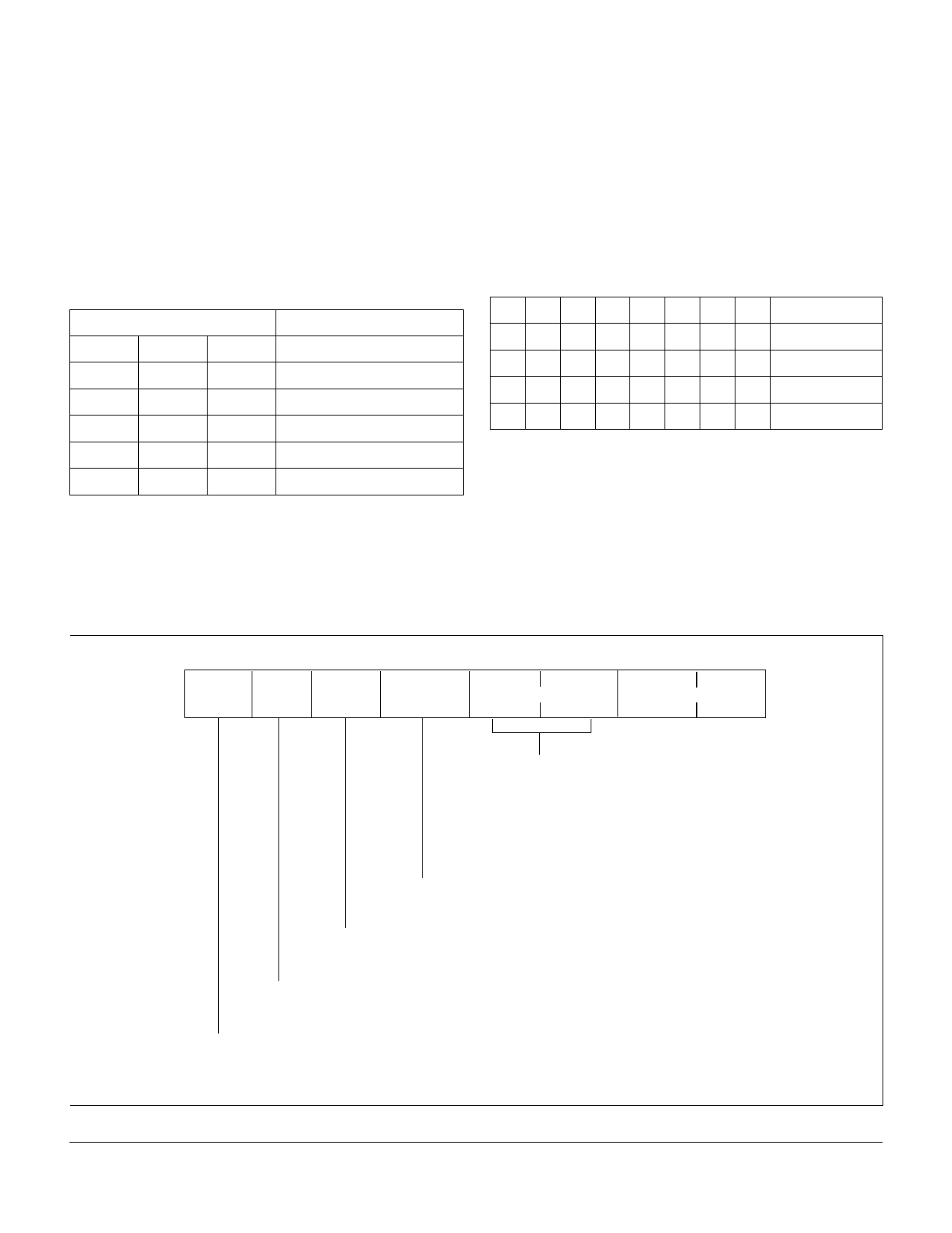
Pin Assignments and Definitions
Pin Function Definition
Pin Function Definition
1 RD
Active low, will enable a processor to read all 11 WR
registers in the display.
Write. Active low. If the device is selected, a
low on the write input loads the data into mem-
ory.
2 CLK I/O If CLK SEL (pin 3) is low, then expect an exter- 12 D7
nal clock source into this pin. If CLK SEL is
high, then this pin will be the master or source
into this pin. If CLK SEL is high, then this pin
will be the master or source for all other
devices which have CLK SEL low.
Data Bus bit 7 (MSB).
3 CLKSEL CLOCK SELECT determines the action of pin 13 D6
2. CLK I/O, see the section on Cascading for
an example.
Data Bus bit 6.
4 RST
Reset. Used to synchronize blinking. Will not
clear the display. The reset pulse should be
less than 1 ms
14 D5
Data Bus bit 5.
5 CE1
6 CE0
Chip enable (active high).
Chip enable (active low).
15 D4
16 D3
Data Bus bit 4.
Data Bus bit 3.
7 A2
8 A1
Address input (MSB).
Address input.
17 D2
18 D1
Data Bus bit 2.
Data Bus bit 1.
9 A0
Address input (LSB).
19 D0
Data Bus bit 0 (LSB).
10 GND
Ground.
20 VCC
Positive power pin.
2006-01-23
7
Share Link: