PM39LV010 查看數據表(PDF) - PMC-Sierra, Inc
零件编号
产品描述 (功能)
生产厂家
PM39LV010 Datasheet PDF : 20 Pages
| |||
PMC
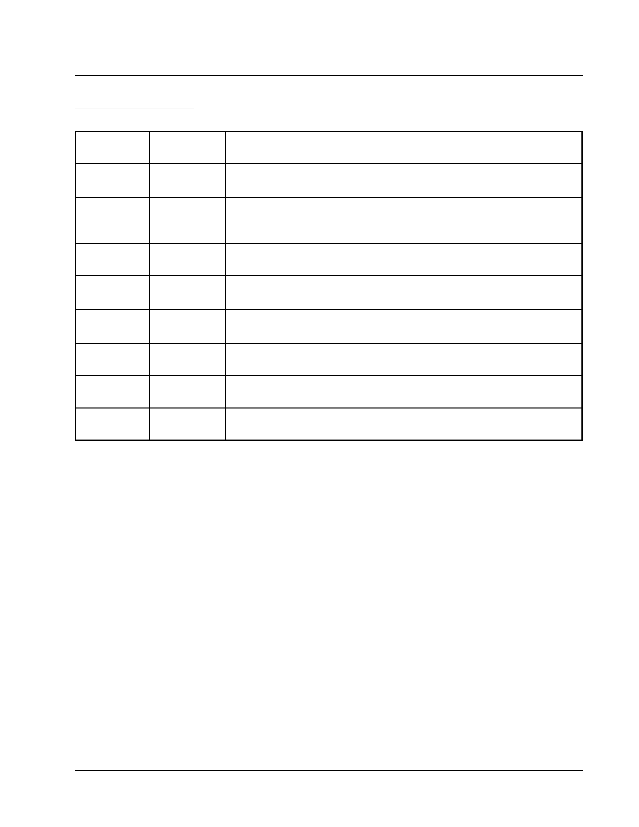
PIN DESCRIPTIONS
Pm39LV512 / Pm39LV010 / Pm39LV020 / Pm39LV040
SYMBOL
A0
-
A (1)
MS
CE#
WE#
OE#
I/O0 - I/O7
VCC
GND
TYPE
DESCRIPTION
INPUT
INPUT
Address Inputs: For memory addresses input. Addresses are internally
latched on the falling edge of WE# during a write cycle.
Chip Enable: CE# goes low activates the device's internal circuitries for
device operation. CE# goes high deselects the device and switches into
standby mode to reduce the power consumption.
INPUT
Write Enable: Activate the device for write operation. WE# is active low.
INPUT
INPUT/
OUTPUT
Output Enable: Control the device's output buffers during a read cycle. OE#
is active low.
Data Inputs/Outputs: Input command/data during a write cycle or output data
during a read cycle. The I/O pins float to tri-state when OE# are disabled.
Device Power Supply
Ground
NC
No Connection
Note:
1. AMS is the most significant address where AMS = A15 for Pm39LV512, A16 for Pm39LV010, A17 for
Pm39LV020, and A18 for Pm39LV040.
Programmable Microelectronics Corp.
4
Issue Date: December, 2003 Rev: 1.2
Share Link: 