MQ80C196KB 查看數據表(PDF) - Intel
零件编号
产品描述 (功能)
生产厂家
MQ80C196KB Datasheet PDF : 30 Pages
| |||
M80C196KB
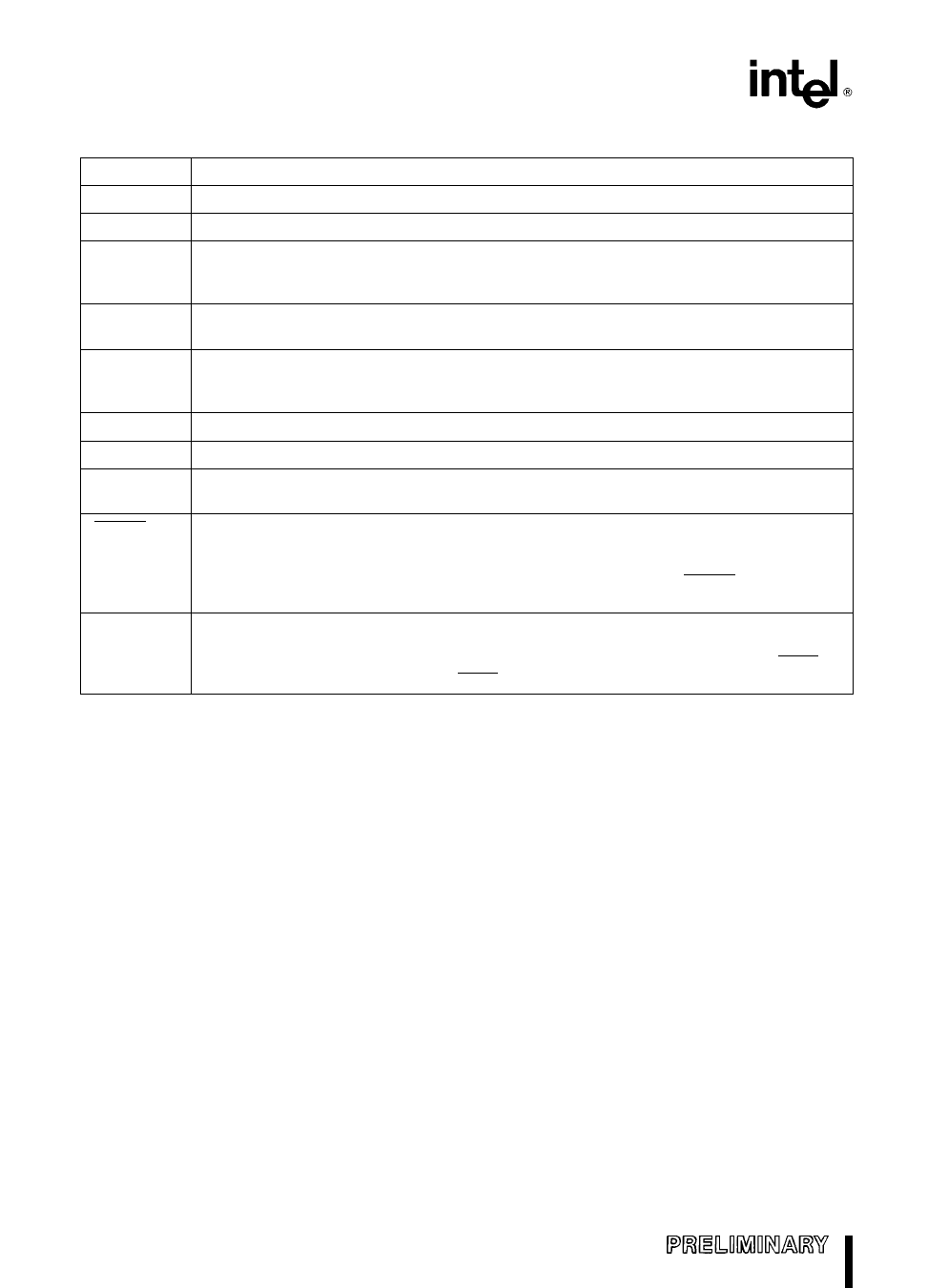
PIN DESCRIPTIONS
Symbol
Name and Function
VCC
VSS
VREF
Main supply voltage (5V)
Digital circuit ground (0V) There are three VSS pins all of which must be connected
Reference voltage for the A D converter (5V) VREF is also the supply voltage to the
analog portion of the A D converter and the logic used to read Port 0 Must be connected
for A D and Port 0 to function
ANGND
VPP
XTAL1
Reference ground for the A D converter Must be held at nominally the same potential as
VSS
Timing pin for the return from powerdown circuit Connect this pin with a 1 mF capacitor to
VSS and a 1 MX resistor to VCC If this function is not used VPP may be tied to VCC This
pin was VBB on the 8X9X-90 parts and is the programming voltage on EPROM part
Input of the oscillator inverter and of the internal clock generator
XTAL2
Output of the oscillator inverter
CLKOUT
Output of the internal clock generator The frequency of CLKOUT is the oscillator
frequency It has a 50% duty cycle
RESET
Reset input to the chip Input low for at least 4 state times to reset the chip The
subsequent low-to-high transition re- synchronizes CLKOUT and commences a 10-state-
time sequence in which the PSW is cleared a byte read from 2018H loads CCR and a
jump to location 2080H is executed Input high for normal operation RESET has an
internal pullup
BUSWIDTH
Input for buswidth selection If CCR bit 1 is a one this pin selects the bus width for the bus
cycle in progress If BUSWIDTH is a 1 a 16-bit bus cycle occurs If BUSWIDTH is a 0 an
8-bit cycle occurs If CCR bit 1 is a 0 the bus is always an 8-bit bus This pin is the TEST
pin on 8X9X-90 parts Systems with TEST tied to VCC do not need to change
8
Share Link: 