AD7846 查看數據表(PDF) - Analog Devices
零件编号
产品描述 (功能)
生产厂家
AD7846 Datasheet PDF : 24 Pages
| |||
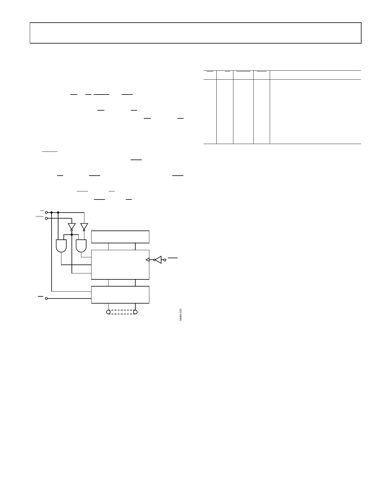
CIRCUIT DESCRIPTION
DIGITAL SECTION
Figure 20 shows the digital control logic and on-chip data latches
in the AD7846. Table 7 is the associated truth table. The digital-
to-analog converter (DAC) has two latches that are controlled
by four signals: CS, R/W, LDAC, and CLR. The input latch is
connected to the data bus (DB15 to DB0). A word is written to
the input latch by bringing CS low and R/W low. The contents
of the input latch can be read back by bringing CS low and R/W
high. This feature is called readback and is used in system
diagnostic and calibration routines.
Data is transferred from the input latch to the DAC latch with
the LDAC strobe. The equivalent analog value of the DAC latch
contents appears at the DAC output. The CLR pin resets the
DAC latch contents to 000…000 or 100…000, depending on the
state of R/W. Writing a CLR loads 000…000 and reading a CLR
loads 100…000. To reset a DAC to 0 V in a unipolar system, the
user should assert CLR while R/W is low; to reset to 0 V in a
bipolar system, assert the CLR while R/W is high.
R/ W
CLR
DAC
16
DB15 RST
DB15 SET
DB15 TO DB0
LATCHES
DB14 TO DB0
RST
16
LDAC
3-STATE I/O
CS
LATCH
16
DB15
DB0
Figure 20. Input Control Logic
AD7846
Table 7. Control Logic Truth Table
CS R/W LDAC CLR Function
1X X
X 3-state DAC I/O latch in high-Z state
00 X
X DAC I/O latch loaded with DB15
to DB0
01 X
X Contents of DAC I/O latch available
on DB15 to DB0
XX 0
1 Contents of DAC I/O latch transferred
to DAC latch
X0 X
0 DAC latch loaded with 000…000
X1 X
0 DAC latch loaded with 100…000
DIGITAL-TO-ANALOG CONVERSION
Figure 21 shows the digital-to-analog section of the AD7846.
There are three DACs, each of which has its own buffer
amplifiers. DAC1 and DAC2 are 4-bit DACs. They share a
16-resistor string but have their own analog multiplexers. The
voltage reference is applied to the resistor string. DAC3 is a
12-bit voltage mode DAC with its own output stage.
The four MSBs of the 16-bit digital code drive DAC1 and DAC2,
and the 12 LSBs control DAC3. Using DAC1 and DAC2, the
MSBs select a pair of adjacent nodes on the resistor string and
present that voltage to the positive and negative inputs of
DAC3. This DAC interpolates between these two voltages to
produce the analog output voltage.
To prevent nonmonotonicity in the DAC due to amplifier offset
voltages, DAC1 and DAC2 leap along the resistor string. For
example, when switching from Segment 1 to Segment 2, DAC1
switches from the bottom of Segment 1 to the top of Segment 2
while DAC2 stays connected to the top of Segment 1. The code
driving DAC3 is automatically complemented to compensate
for the inversion of its inputs. This means that any linearity
effects due to amplifier offset voltages remain unchanged when
switching from one segment to the next and 16-bit monotonicity is
ensured if DAC3 is monotonic. Thus, 12-bit resistor matching
in DAC3 guarantees overall 16-bit monotonicity. This is much
more achievable than 16-bit matching, which a conventional
R-2R structure needs.
Rev. G | Page 11 of 24
Share Link: 