SST58LM128 查看數據表(PDF) - Silicon Storage Technology
零件编号
产品描述 (功能)
生产厂家
SST58LM128 Datasheet PDF : 40 Pages
| |||
ATA-Disk Module
SST58SM008 / 016 / 024 / 032 / 048 / 064 / 096 / 128 / 192
SST58LM008 / 016 / 024 / 032 / 048 / 064 / 096 / 128 / 192
Advance Information
TABLE 2-3: SIGNAL DESCRIPTION
Symbol
Type1 Pin
A2 - A0
I 33,34,35
D15 - D0
I/O 18,16,14,12,10,
8,6,4,3,5,7,9,11,
13,15,17
CS1FX#, CS3FX#
I 37,38
CSEL
- 28
IORD#
IOWR#
IOCS16#
INTRQ
PDIAG#
DASP#
RESET#
GND
WP#3
I 25
I 23
O 32
O 31
I/O 34
I/O 39
I1
- 2,19,22,24,26,
30,40,432
I 30
VDD
- 204, 412, 422
1. Please refer to Sections 2.3.1 to 2.3.4 for detail
2. Only available with the 44-pin connector module
3. Pin 30 is jumper selectable as NC or WP#
4. Only available with the 40-pin connector module
Name and Functions
A[2:0] are used to select one of the Task File registers.
Data bus
CS1FX# is the chip select for the task file registers while CS3FX# is used to
select the Alternate Status Register and the Device Control Register.
CSEL signal is a NC to the motherboard. The Master/Slave selection is set by a
jumper. If the jumper is in a Master position, the ADM is addressed as a Master
drive, and if the jumper is in a Slave position, the ADM is addressed as a Slave
drive.
This is an I/O Read strobe generated by the host. This signal gates I/O data
onto the bus from the chip.
The I/O Write strobe pulse is used to clock I/O data into the chip.
This output signal is asserted low when this device is expecting a word data
transfer cycle.
Signal is the active high Interrupt Request to the host.
This input/output is the Pass Diagnostic signal in the Master/Slave hand-
shake protocol.
This input/output is the Disk Active/Slave present signal in the Master/Slave
handshake protocol.
This input pin is the active low hardware reset from the host.
Ground
Write protect pin is used to disable Write operation. The 3-position jumper can set
pin 30 as NC, write protected (by connecting to GND), or host selectable (by con-
necting to pin 30 of IDE connector). When the signal on this pin is low, data on the
chip will be write-protected. (See Figure 2-1)
Power
T2-3.6 519
For the 40-pin ATA-Disk Module, power can be supplied either through the pin 20 (not present on standard 40-pin
IDE interface) or through the external power connector provided on the 40-pin ADM. Please see the drawings in
“Physical Dimensions” on page 36 for information.
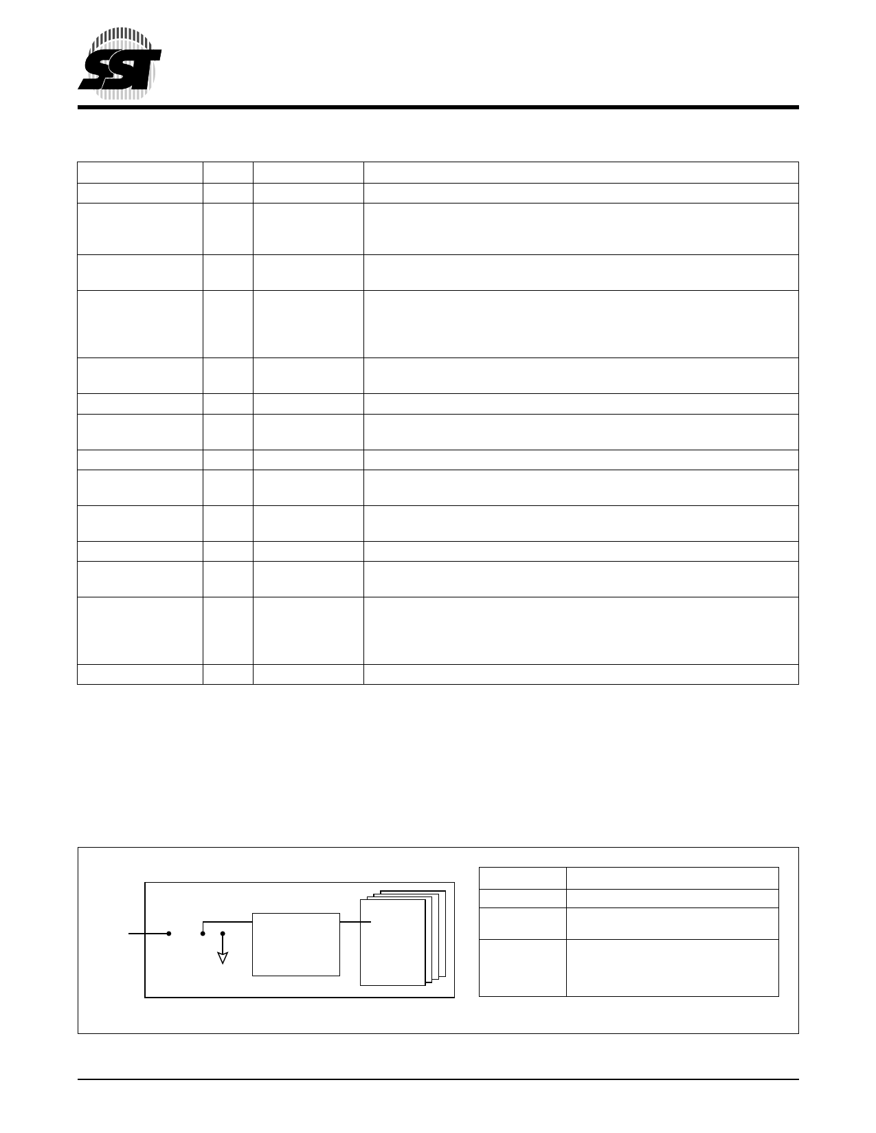
Pin 30
ATA-Disk Module
WP# Jumper
3
21
ATA Controller
FIGURE 2-1: PIN 30 CONFIGURATION
Flash
Memory
519 ILL2-5.1
WP# Jumper ATA-Disk Module
No Jumper
NC, Module is NOT write protected.
Close 1, 2
Connect to Ground,
Module is write protected
Close 2, 3
Host Selectable,
Module is write protected if pin 30 is low.
Module is NOT write protected if pin 30
is high.
T2-3.0 519
©2001 Silicon Storage Technology, Inc.
8
S71193-01-000 9/01 519
Share Link: 