M66004FP 查看數據表(PDF) - MITSUBISHI ELECTRIC
零件编号
产品描述 (功能)
生产厂家
M66004FP Datasheet PDF : 14 Pages
| |||
MITSUBISHI 〈DIGITAL ASSP〉
M66004SP/FP
16-DIGIT 5X7-SEGMENT VFD CONTROLLER
7. Write to character RAM for user definition
Segment ON/OFF data is written into the character RAM for
user definition (35 bits). After write to RAM is declared at the
first byte, RAM is selected at the second byte and ON/OFF
data is transmitted at the 3rd to 7th byte. Therefore, write to
RAM is executed by a 7-byte command.
Character codes from RAM1 to RAM 16 are assigned to data
from 9016 to 9F16 respectively.
D7 D6 D5 D4 D3 D2 D1 D0
1st byte
(Declaration of 1 1 1 1 1 1 × ×
write to RAM)
× : Don’t care
D7 D6 D5 D4 D3 D2 D1 D0
2nd byte
(Selection of RAM)
×
×
×
×
RAM selection
RAM 1 : (D3, D2, D1, D0) = (0, 0, 0, 0)
RAM 16: (D3, D2, D1, D0) = (1, 1, 1, 1)
× : Don’t care
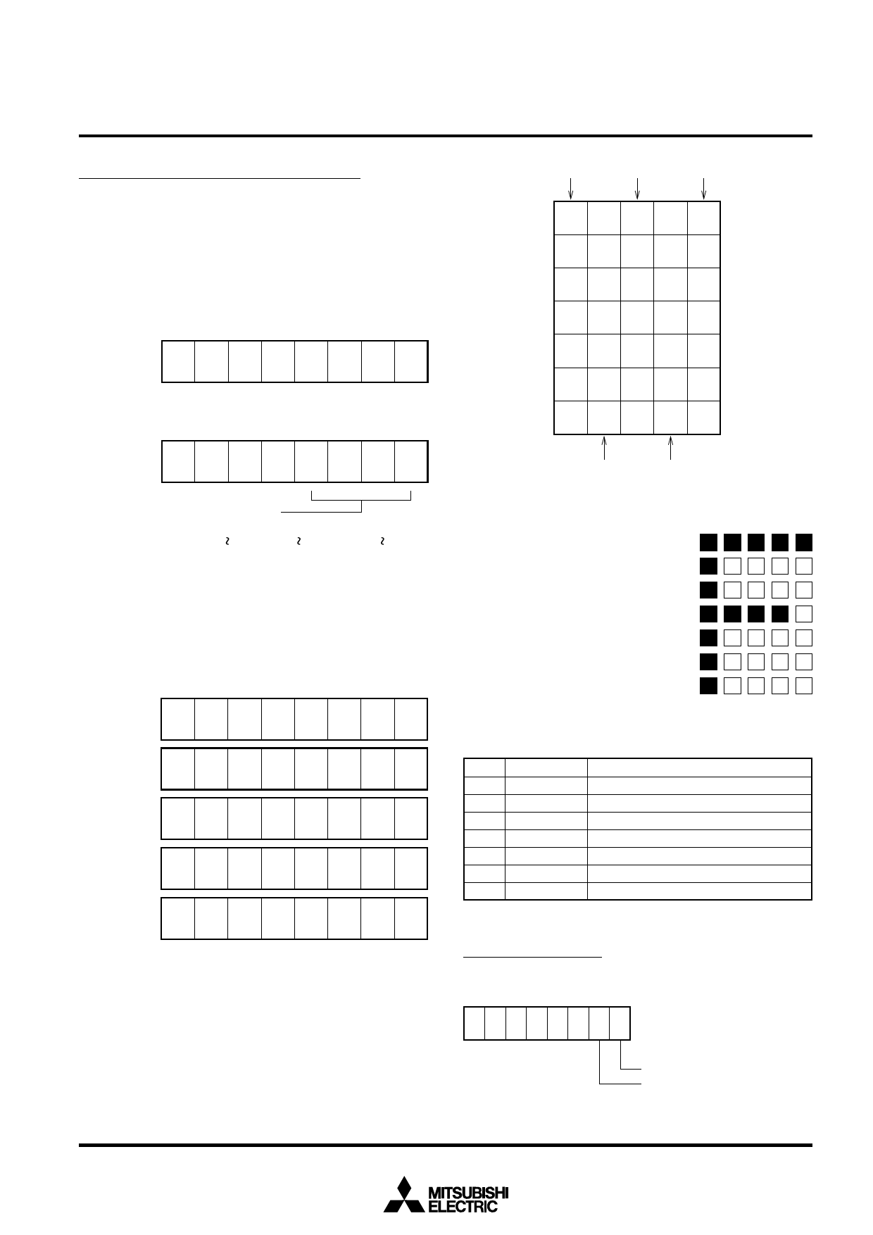
1st column 3rd column 5th column
00 01 02 03 04
05 06 07 08 09
10 11 12 13 14
15 16 17 18 19
20 21 22 23 24
25 26 27 28 29
30 31 32 33 34
2nd column 4th column
(Segment number)
Ex. In order to define “F” (see the figure) as
character RAM 1, 7-byte data as shown
in the following table should be
transmitted in serial order.
D7 D6 D5 D4 D3 D2 D1 D0
3rd byte (Data
in 1st column) 00 05 10 15 20 25 30 ×
4th byte (Data
in 2nd column) 01 06 11 16 21 26 31 ×
5th byte (Data
in 3rd column) 02 07 12 17 22 27 32 ×
6th byte (Data
in 4th column) 03 08 13 18 23 28 33 ×
7th byte (Data
in 5th column) 04 09 14 19 24 29 34 ×
0: corresponding segment OFF
1: corresponding segment ON
Transmission data
Remarks
1
FC16
Declaration of write to RAM 1
2
0016
Selection of RAM 1
3
FE16
Setting of 1st-column segment data
4
9016
Setting of 2nd-column segment data
5
9016
Setting of 3rd-column segment data
6
9016
Setting of 4th-column segment data
7
8016
Setting of 5th-column segment data
All optional bits are set to “0”.
8. Output port setting
D7 D6 D5 D4 D3 D2 D1 D0
111110
P0 set/reset
P1 set/reset
Set (“H”): 1
Reset (“L”): 0
7
Share Link: 