UPA1700AG-E1 查看數據表(PDF) - NEC => Renesas Technology
零件编号
产品描述 (功能)
生产厂家
UPA1700AG-E1 Datasheet PDF : 8 Pages
| |||
µPA1700A
ELECTRICAL CHARACTERISTICS (TA = 25 ˚C, all terminals are connected)
CHARACTERISTICS
SYMBOL
Drain to Source On-state Resistance RDS(on)1
RDS(on)2
Gate to Source Cutoff Voltage
VGS(off)
Forward Transfer Admittance
|yfs|
Drain Leakage Current
IDSS
Gate to Source Leakage Current
IGSS
Input Capacitance
Ciss
Output Capacitance
Coss
Reverse Transfer Capacitance
Crss
Turn-On Delay Time
td(on)
Rise Time
tr
Turn-Off Delay Time
td(off)
Fall Time
tf
Total Gate Charge
QG
Gate to Source Charge
QGS
Gate to Drain Charge
QGD
Body Diode Forward Voltage
VF(S-D)
Reverse Recovery Time
trr
Reverse Recovery Charge
Qrr
TEST CONDITIONS
VGS = 10 V, ID = 3.5 A
VGS = 4 V, ID = 3.5 A
VDS = 10 V, ID = 1 mA
VDS = 10 V, ID = 3.5 A
VDS = 30 V, VGS = 0
VGS = ±20 V, VDS = 0
VDS = 10 V
VGS = 0
f = 1 MHz
ID = 3.5 A
VGS(on) = 10 V
VDD = 15 V
RG = 10 Ω
ID = 7.0 A
VDD = 24 V
VGS = 10 V
IF = 7.0 A, VGS = 0
IF = 7.0 A, VGS = 0
di/dt = 100 A/µs
MIN.
1.0
5.0
TYP.
18
28
1.6
9.0
820
350
160
18
98
57
32
20
2.4
5.6
0.79
36
35
MAX.
27
50
2.0
10
±10
UNIT
mΩ
mΩ
V
S
µA
µA
pF
pF
pF
ns
ns
ns
ns
nC
nC
nC
V
ns
nC
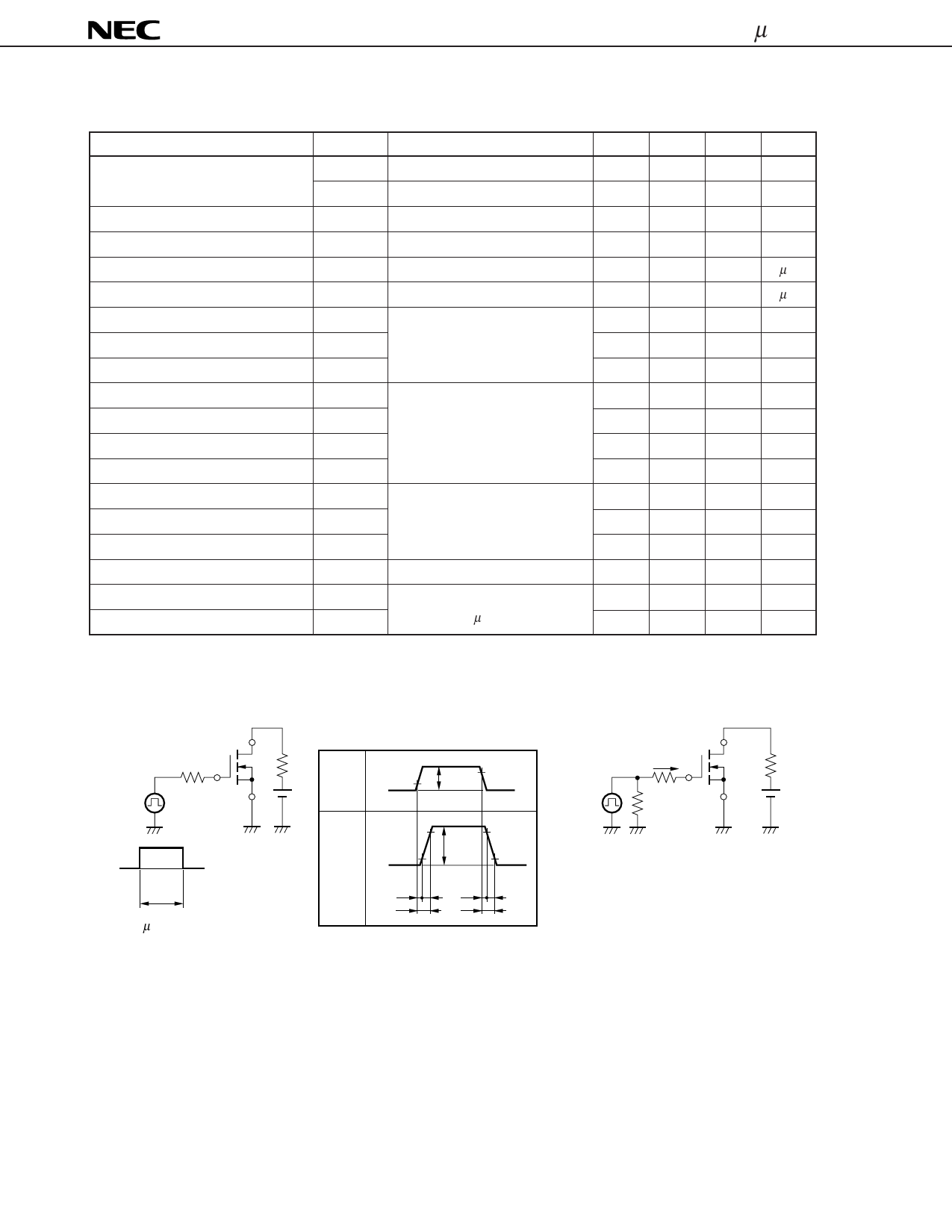
Test Circuit 1 Switching Time
D.U.T.
RG
PG. RG = 10 Ω
VGS
0
t
t = 1 µs
Duty Cycle ≤ 1 %
RL
VDD
VGS
VGS
Wave Form
10 %
0
VGS(on)
ID
90 %
ID
Wave Form
0 10 %
td(on)
ID
tr
td(off)
90 %
90 %
10 %
tf
ton
toff
Test Circuit 2 Gate Charge
D.U.T.
IG = 2 mA
RL
PG.
50 Ω
VDD
2
Share Link: 