UPA1800GR-9JG 查看數據表(PDF) - NEC => Renesas Technology
零件编号
产品描述 (功能)
生产厂家
UPA1800GR-9JG Datasheet PDF : 8 Pages
| |||
µ PA1800
5 ELECTRICAL CHARACTERISTICS (TA = 25 °C)
CHARACTERISTICS
SYMBOL
TEST CONDITIONS
Zero Gate Voltage Drain Current
IDSS
VDS = 30 V, VGS = 0 V
Gate Leakage Current
IGSS
VGS = ±20 V, VDS = 0 V
Gate Cut-off Voltage
VGS(off) VDS = 10 V, ID = 1 mA
Forward Transfer Admittance
| yfs | VDS = 10 V, ID = 3.0 A
Drain to Source On-state Resistance
RDS(on)1 VGS = 10 V, ID = 3.0 A
RDS(on)2 VGS = 4.5 V, ID = 3.0 A
RDS(on)3 VGS = 4.0 V, ID = 3.0 A
Input Capacitance
Ciss
VDS = 10 V
Output Capacitance
Coss
VGS = 0 V
Reverse Transfer Capacitance
Crss
f = 1 MHz
Turn-on Delay Time
td(on)
VDD = 15 V
Rise Time
tr
ID = 3.0 A
Turn-off Delay Time
td(off)
VGS(on) = 10 V
Fall Time
tf
RG = 10 Ω
Total Gate Charge
QG
VDD = 24 V
Gate to Source Charge
QGS ID = 5.0 A
Gate to Drain Charge
QGD
VGS = 10 V
Diode Forward Voltage
VF(S-D) IF = 5.0 A, VGS = 0 V
Reverse Recovery Time
Reverse Recovery Charge
trr
IF = 5.0 A, VGS = 0 V
Qrr
di/dt = 100 A/µs
MIN. TYP. MAX. UNIT
10 µA
±10 µA
1.0 1.41 2.0 V
3.0 7.0
S
20 27 mΩ
29 39 mΩ
32 45 mΩ
680
pF
470
pF
170
pF
18
ns
70
ns
60
ns
26
ns
23
nC
2
nC
7
nC
0.74
V
60
ns
80
nC
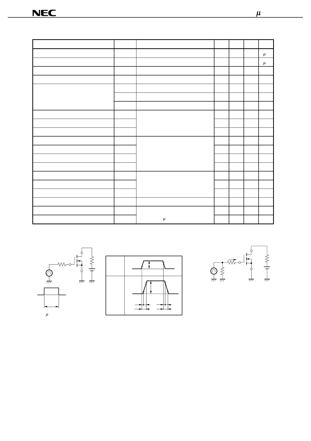
TEST CIRCUIT 1 SWITCHING TIME
TEST CIRCUIT 2 GATE CHARGE
D.U.T.
RG
PG.
VGS
0
τ
τ = 1µs
Duty Cycle ≤ 1 %
RL
VGS
VGS
Wave Form
010 %
VGS(on) 90 %
VDD
ID
90 %
ID
ID
0 10 %
Wave Form
90 %
10 %
td(on) tr td(off) tf
ton
toff
D.U.T.
IG = 2 mA
RL
PG.
50 Ω
VDD
2
Data Sheet D11407EJ1V0DS00
Share Link: 