UPD6121 查看數據表(PDF) - NEC => Renesas Technology
零件编号
产品描述 (功能)
生产厂家
UPD6121 Datasheet PDF : 28 Pages
| |||
µPD6121, 6122
* 3.2 Standard versions with Ver II specs. (µPD6121-002, 6122-002)
In Ver II, the CCS pin does not have the external diode reading function.
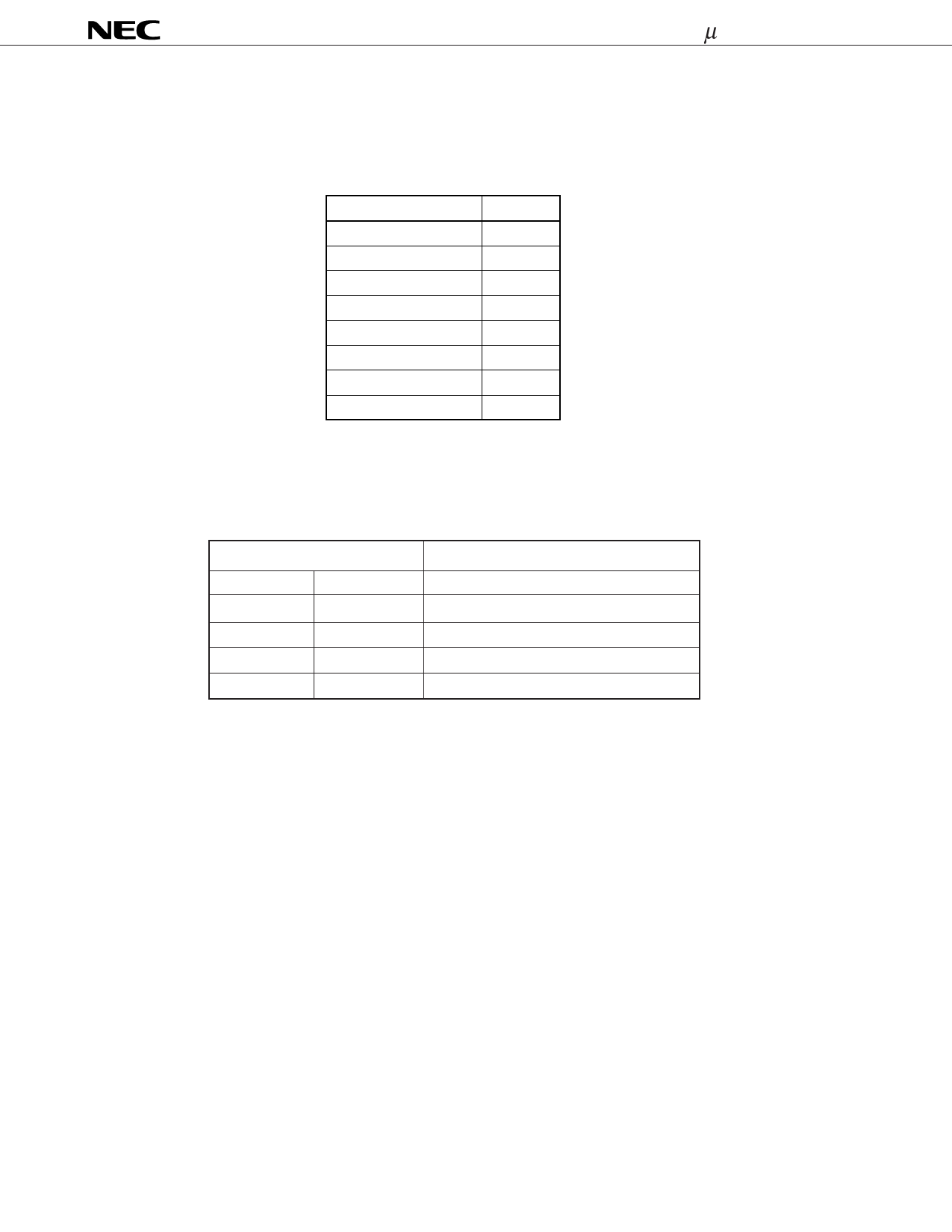
The allocation of C2, C1 and C0 of the higher 8 bits of the custom code is done by connecting the CCS pin
to any one of the KI/O0 to KI/O7 pins, as shown below.
Pin connected to CCS pin C2 C1 C0
KI/O0
000
KI/O1
001
KI/O2
010
KI/O3
011
KI/O4
100
KI/O5
101
KI/O6
110
KI/O7
111
When CCS pin is open, (C2 C1 C0) = (0 0 0)
*
The allocation of C7, C6, C5, C4 and C3 of the higher 8 bits of the custom code is as follows depending on
whether a pull-up resistor is provided.
Pull-up Resistor
KI/O6
Not Provided
KI/O7
Not Provided
Not Provided
Provided
Provided
Not Provided
Provided
Provided
C7 to C3 of Higher 8 bits of Custom Code
C7
C6
C5
0
0
0
C4
C3
0
0
1
0
0
1
1
1
0
0
0
0
1
1
1
0
1
Caution
In Ver II, it is not possible to set all custom codes.
Also, new custom codes cannot be ordered for Ver II products; therefore, Ver I products should
be used if new custom codes are required.
8
Share Link: 