VSC7216UC-01 查看數據表(PDF) - Vitesse Semiconductor
零件编号
产品描述 (功能)
生产厂家
VSC7216UC-01 Datasheet PDF : 38 Pages
| |||
VITESSE
SEMICONDUCTOR CORPORATION
Multi-Gigabit Interconnect Chip
Multi-Gigabit Interconnect Chip
Preliminary Data Sheet
VSCV7S2C1672-0116
When used, the TBCn inputs must be frequency-locked to REFCLK. No phase relationship is assumed. A
small skew buffer is provided to tolerate phase drift between TBCn and REFCLK. This buffer is recentered by
the RESETN input, and the total phase drift after recentering must be limited to ±180° (where 360° is one
character time). Each channel has an error output, TBERRn, that is asserted HIGH to indicate that the phase
drift between TBCn and REFCLK has accumulated to the point that the elastic limit of the skew buffer has been
exceeded and a transmit data character has been either dropped or duplicated. This error can not occur when
input timing is referenced to REFCLK. The TBERRn output timing is identical to the low-speed receiver
outputs, as selected by RMODE(1:0) in Table 6.
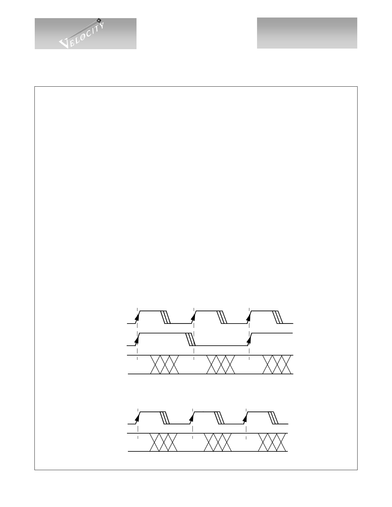
Figures 2 through 4 show the possible relationships between data and control inputs and the selected input
timing source. Figure 2 shows how REFCLK is used as an input timing reference. This mode of operation is
used in the VSC7211 and VSC7214. Figure 3 and Figure 4 show how TBCn is used as an input timing
reference. When TBCn is used to define a data eye as shown in Figure 4, it functions as an additional data input
that simply toggles every cycle.
Note that the REFCLK and TBCn inputs are not used directly to clock the input data. Instead, an internal
Phase-Lock Loop (PLL) generates edges aligned with the appropriate clock. The arrows on the rising edges of
these signals define the reference edge for the internal phase detection logic. An internal clock is generated at
one-tenth the serial transmit data rate that is locked to the selected input timing source. This is an especially
important issue when DUAL is HIGH and input timing is referenced to REFCLK, since the falling edge is NOT
used. The internal clock active edges are placed coincident with the REFCLK rising edges and halfway between
the REFCLK rising edges in this mode.
A similar situation exists when TBCn is used to define a data eye, only the rising edges of TBCn are used to
define the external data timing. The internal clock active edges are placed at 90° and 270° points between
consecutive TBCn rising edges (which are assumed to be 360° apart).
Figure 2: Transmit Timing, TMODE(2:0) = 000
REFCLK
(DUAL = 0)
REFCLK
(DUAL = 1)
Tn(7:0)
C/Dn
Valid
WSENn
Valid
Valid
Figure 3: Transmit Timing, TMODE(2:0) = 10X
TBCA
or
TBCn
Tn(7:0)
C/Dn
Valid
WSENn
Valid
Valid
Page 4
© VITESSE SEMICONDUCTOR CORPORATION • 741 Calle Plano • Camarillo, CA 93012
Tel: (800) VITESSE • FAX: (805) 987-5896 • Email: prodinfo@vitesse.com
Internet: www.vitesse.com
G52352-0, Rev 3.2
05/05/01
Share Link: 