WED2ZL361MS38BC 查看數據表(PDF) - White Electronic Designs Corporation
零件编号
产品描述 (功能)
生产厂家
WED2ZL361MS38BC Datasheet PDF : 12 Pages
| |||
White Electronic Designs
WED2ZL361MS
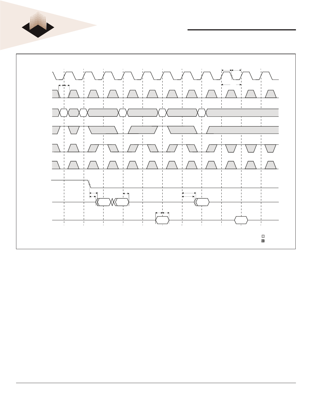
FIG. 6 TIMING WAVEFORM OF CE# OPERATION
Clock
CKE#
tCSS tCSH
Address
A1
A2
A3
A4
A5
WRITE#
CEx#
ADV
OE#
Data Out
Data In
tLZtOOEE
Q1
tHZC
Q2
ttLCZDC
Q4
tDS tDH
D3
NOTES:
WRITE# = L means WE# = L, and BWx# = L
CEx# refers to the combination of CE1#, CE2 and CE2#.
tCH tCL
tCYC
D5
Dont Care
Undefined
White Electronic Designs Corp. reserves the right to change products or specifications without notice.
Oct, 2002
Rev. 5
11
White Electronic Designs Corporation • (602) 437-1520 • www.wedc.com
Share Link: 