WED2ZL361MS42BI 查看數據表(PDF) - White Electronic Designs Corporation
零件编号
产品描述 (功能)
生产厂家
WED2ZL361MS42BI Datasheet PDF : 12 Pages
| |||
White Electronic Designs
WED2ZL361MS
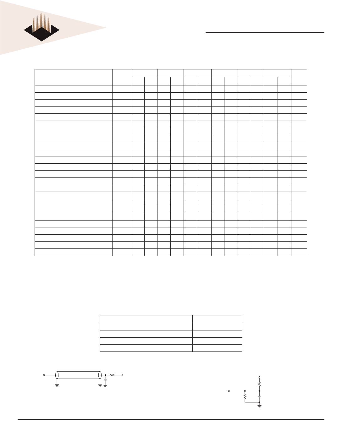
AC CHARACTERISTICS
Parameter
250MHz
225MHz
200MHz
166MHz
150MHz
133MHz
Symbol
Units
Min Max Min Max Min Max Min Max Min Max Min Max
Clock Time
tCYC
4.0
4.4
5.0
6.0
6.7
7.5
ns
Clock Access Time
tCD
-- 2.6 -- 2.8 -- 3.0 -- 3.5 -- 3.8 -- 4.2 ns
Output enable to Data Valid
tOE
-- 2.6 -- 2.8 -- 3.0 -- 3.5 -- 3.8 -- 4.2 ns
Clock High to Output Low-Z
tLZC 1.5 -- 1.5 -- 1.5 -- 1.5 -- 1.5 -- 1.5 --
ns
Output Hold from Clock High
tOH
1.5 -- 1.5 -- 1.5 -- 1.5 -- 1.5 -- 1.5 --
ns
Output Enable Low to output Low-Z
tLZOE 0.0 -- 0.0 -- 0.0 -- 0.0 -- 0.0 -- 0.0 --
ns
Output Enable High to Output High-Z
tHZOE -- 2.6 -- 2.8 -- 3.0 -- 3.0 -- 3.0 -- 3.5 ns
Clock High to Output High-Z
tHZC
-- 2.6 -- 2.8 -- 3.0 -- 3.0 -- 3.0 -- 3.5 ns
Clock High Pulse Width
tCH
1.7 -- 2.0 -- 2.0 -- 2.2 -- 2.2 -- 2.2 --
ns
Clock Low Pulse Width
tCL
1.7 -- 2.0 -- 2.0 -- 2.2 -- 2.2 -- 2.2 --
ns
Address Setup to Clock High
tAS
1.2 -- 1.4 -- 1.4 -- 1.5 -- 1.5 -- 1.5 --
ns
CKE Setup to Clock High
tCES 1.2 -- 1.4 -- 1.4 -- 1.5 -- 1.5 -- 1.5 --
ns
Data Setup to Clock High
tDS
1.2 -- 1.4 -- 1.4 -- 1.5 -- 1.5 -- 1.5 --
ns
Write Setup to Clock High
tWS
1.2 -- 1.4 -- 1.4 -- 1.5 -- 1.5 -- 1.5 --
ns
Address Advance to Clock High
tADVS 1.2 -- 1.4 -- 1.4 -- 1.5 -- 1.5 -- 1.5 --
ns
Chip Select Setup to Clock High
tCSS 1.2 -- 1.4 -- 1.4 -- 1.5 -- 1.5 -- 1.5 --
ns
Address Hold to Clock high
tAH
0.3 -- 0.4 -- 0.4 -- 0.5 -- 0.5 -- 0.5 --
ns
CKE Hold to Clock High
tCEH 0.3 -- 0.4 -- 0.4 -- 0.5 -- 0.5 -- 0.5 --
ns
Data Hold to Clock High
tDH
0.3 -- 0.4 -- 0.4 -- 0.5 -- 0.5 -- 0.5 --
ns
Write Hold to Clock High
tWH
0.3 -- 0.4 -- 0.4 -- 0.5 -- 0.5 -- 0.5 --
ns
Address Advance to Clock High
tADVH 0.3 -- 0.4 -- 0.4 -- 0.5 -- 0.5 -- 0.5 --
ns
Chip Select Hold to Clock High
tCSH 0.3 -- 0.4 -- 0.4 -- 0.5 -- 0.5 -- 0.5 --
ns
ZZ High to Power Down
tPDS
2 -- 2 --
2
--
2 -- 2 --
2
-- cycle
ZZ Low to Power Up
tPUS
2 -- 2 --
2
--
2 -- 2 --
2
-- cycle
NOTES:
1. All Address inputs must meet the specified setup and hold times for all rising clock (CK) edges when ADV is sampled low and CEx# is sampled valid. All other
synchronous inputs must meet the specified setup and hold times whenever this device is chip selected.
2. Chip enable must be valid at each rising edge of CK (when ADV is Low) to remain enabled.
3. A write cycle is defined by WE# low having been registered into the device at ADV Low. A Read cycle is defined by WE# High with ADV Low. Both cases must
meet setup and hold times.
AC TEST CONDITIONS
(0 ≤ TA ≤ 70°C, VCC = 2.5V ± 5%; Commercial or -40°C ≤ Ta ≤ 85°C; VCC = 2.5V ± 5%; Industrial)
Parameter
Input Pulse Level
Input Rise and Fall Time (Measured at 20% to 80%)
Input and Output Timing Reference Levels
Output Load
Value
0 to 2.5V
1.0V/ns
1.25V
See Output Load (A)
OUTPUT LOAD (A)
Dout
Zo=50Ω
RL=50Ω
30pF*
VL=1.25V
OUTPUT LOAD (B)
(for tLZC, tLZOE, tHZOE, and tHZC)
+2.5V
Dout
1667Ω
1538Ω
5pF*
*Including Scope and Jig Capacitance
White Electronic Designs Corp. reserves the right to change products or specifications without notice.
Oct, 2002
Rev. 5
5
White Electronic Designs Corporation • (602) 437-1520 • www.wedc.com
Share Link: 