WED2DL32512V40BC 查看數據表(PDF) - White Electronic Designs Corporation
零件编号
产品描述 (功能)
生产厂家
WED2DL32512V40BC Datasheet PDF : 9 Pages
| |||
WED2DL32512V
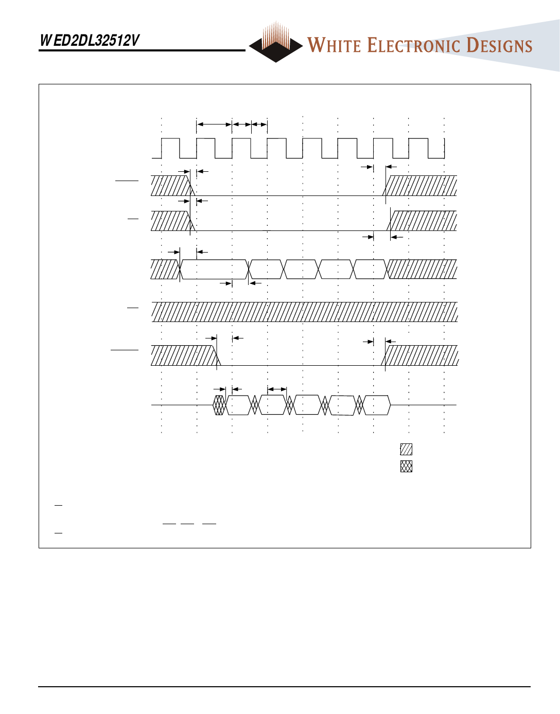
FIG. 4 WRITE TIMING DIAGRAM
tKHK H
tKHK L tKLKH
CLK
ADSC
tSC VKH
tEVKH
CE
ADDR
tAVKH
A1
tKHAX
A2
A3
tKHSCX
tKHEX
A4
A5
OE
WRITE
t WVKH
t KHWX
KHG WX
DQ
tDVK H
tKHDX
D(A1) D(A2)
D(A3)
D (A4)
D(A5)
DON’T CARE
UNDEFINED
NOTES:
1. D (A2) refers to output from address A2. D (A2+1) refers to output from the next internal burst address following A2.
2. OE must be HIGH before the input data setup and held HIGH throughout the data hold time. This prevents input/output data content in for the time period
prior to the byte write enable inputs being sampled.
3. Full-width WRITE can be initiated by BWE, BWa, - BWd LOW. Timing is shown assuming that the device was not enabled before entering into its sequence.
OE does not cause Q to be driven until after the following clock rising edge.
White Electronic Designs Corporation • (508) 366-5151 • www.whiteedc.com
8
Share Link: 