WED3DG644V-D1 查看數據表(PDF) - White Electronic Designs Corporation
零件编号
产品描述 (功能)
生产厂家
WED3DG644V-D1 Datasheet PDF : 8 Pages
| |||
White Electronic Designs
WED3DG644V-D1
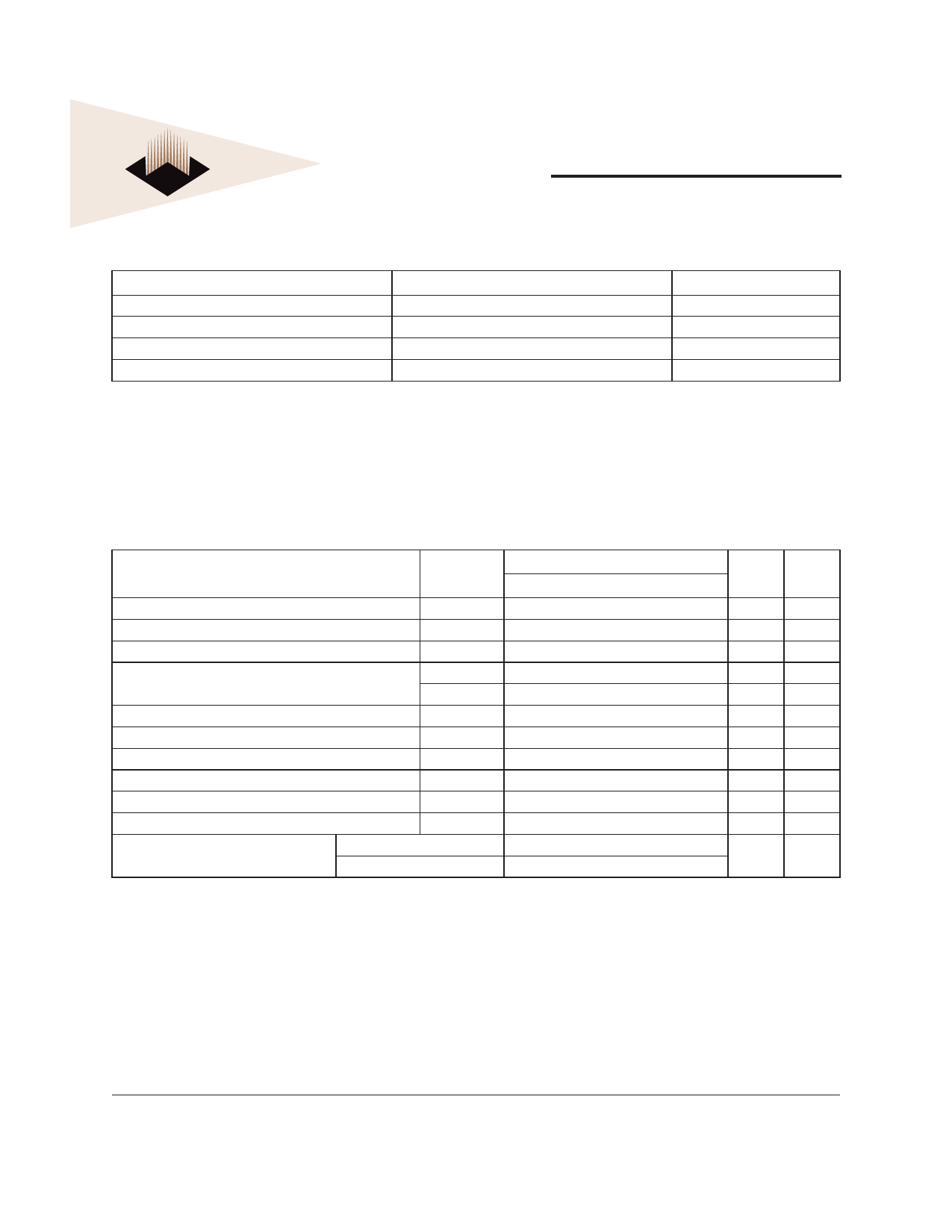
AC OPERATING TEST CONDITIONS
VCC = 3.3V ± 0.3V, 0 ≤ TA ≤ 70°C
Parameter
Value
Unit
AC input levels (VIH/VIL)
2.4/0.4
V
Input timing measurement reference level
1.4
V
Input rise and fall time
tR/tF = 1/1
ns
Output timing measurement reference level
1.4
V
OPERATING AC PARAMETER
(AC operating conditions unless otherwise noted)
Parameter
Row active to row active delay
RAS# to CAS# delay
Row precharge time
Row active time
Row cycle time
Last data in to row precharge
Last data in to Active delay
Last data in to new col. address delay
Last data in to burst stop
Col. address to col. address delay
Number of valid output data
Symbol
tRRD (min)
tRCD (min)
tRP (min)
tRAS (min)
tRAS (max)
tRC (min)
tRDL (min)
tDAL (min)
tCDL (min)
tBDL (min)
tCCD (min)
CAS latency=3
CAS latency=2
Version
7.5, 10
15
20
20
45
100
65
2
2 CLK + tRP
1
1
1
2
1
Unit
Note
ns
1
ns
1
ns
1
ns
1
us
ns
1
CLK
2
—
CLK
2
CLK
2
CLK
3
ea
4
Notes :
1. The minimum number of clock cycles is determined by dividing the minimum time required with clock cycle time and then rounding off to the next higher integer.
2. Minimum delay is required to complete write.
3. All parts allow every cycle column address change.
4. In case of row precharge interrupt, auto precharge and read burst stop.
June 2006
Rev. 3
5
White Electronic Designs Corporation • (602) 437-1520 • www.wedc.com
Share Link: 