WED3DG6419V7D2 查看數據表(PDF) - White Electronic Designs Corporation
零件编号
产品描述 (功能)
生产厂家
WED3DG6419V7D2 Datasheet PDF : 6 Pages
| |||
White Electronic Designs
WED3DG6419V-D2
128MB - 16Mx64 SDRAM UNBUFFERED
FEATURES
Burst Mode Operation
Auto and Self Refresh capability
LVTTL compatible inputs and outputs
Serial Presence Detect with EEPROM
Fully synchronous: All signals are registered on the positive
edge of the system clock
Programmable Burst Lengths: 1, 2, 4, 8 or Full Page
3.3 volt ± 0.3v Power Supply
168 pin DIMM JEDEC
DESCRIPTION
The WED3DG6419V is a 16Mx64 synchronous DRAM module which
consists of sixteen 8Mx8 SDRAM components in TSOP II package
and one 2K EEPROM in an 8 pin TSSOP package for Serial Pres-
ence Detect which are mounted on a 168 pin DIMM multilayer FR4
Substrate.
* This product is subject to change without notice.
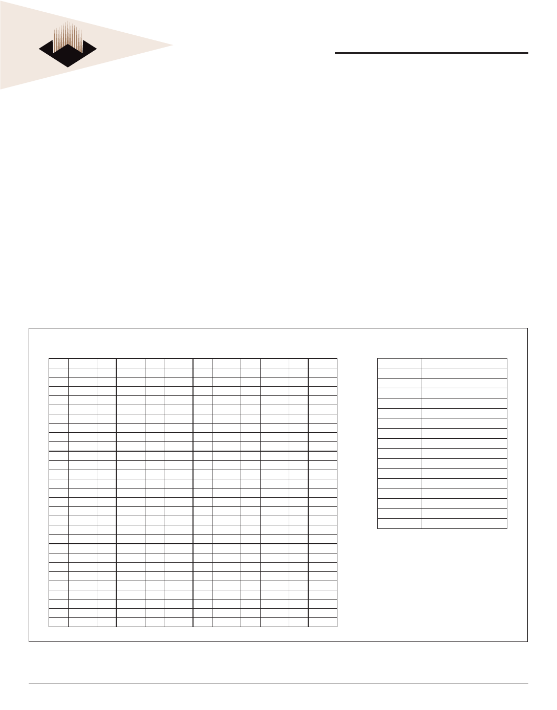
PIN CONFIGURATIONS (FRONT SIDE/BACK SIDE)
Pin Front Pin Front Pin Front Pin Back Pin Back Pin
1
VSS
29 DQM1 57 DQ18 85
VSS
113 DQM5 141
2
DQ0 30 CS0# 58 DQ19 86 DQ32 114 CS1# 142
3
DQ1 31 DNU 59
VCC
87 DQ33 115 RAS# 143
4
DQ2 32
VSS
60 DQ20 88 DQ34 116 VSS 144
5
DQ3 33
A0
61
NC
89 DQ35 117
A1
145
6
VCC
34
A2
62
*VREF
90
VCC
118
A3
146
7
DQ4 35
A4
63 CKE1 91 DQ36 119
A5
147
8
DQ5 36
A6
64
VSS
92 DQ37 120
A7
148
9
DQ6 37
A8
65 DQ21 93 DQ38 121
A9
149
10 DQ7 38 A10/AP 66 DQ22 94 DQ39 122 BA0 150
11 DQ8 39 BA1 67 DQ23 95 DQ40 123 A11 151
12
VSS
40
VCC
68
VSS
96
VSS
124
VCC
152
13
DQ9
41
VCC
69 DQ24 97 DQ41 125 CLK1 153
14 DQ10 42 CLK0 70 DQ25 98 DQ42 126 *A12 154
15 DQ11 43
VSS
71 DQ26 99 DQ43 127 VSS 155
16 DQ12 44 DNU 72 DQ27 100 DQ44 128 CKE0 156
17 DQ13 45 CS2# 73
VCC 101 DQ45 129 CS3# 157
18
VCC
46 DQM2 74 DQ28 102 VCC 130 DQM6 158
19 DQ14 47 DQM3 75 DQ29 103 DQ46 131 DQM7 159
20 DQ15 48 DNU 76 DQ30 104 DQ47 132 *A13 160
21 *CB0 49
VCC
77 DQ31 105 *CB4 133 VCC 161
22 *CB1 50
NC
78
VSS
106 *CB5 134
NC
162
23
VSS
51
NC
79 CLK2 107
VSS
135
NC
163
24
NC
52 *CB2 80
NC 108 NC 136 *CB6 164
25
NC
53 *CB3 81
NC 109 NC 137 *CB7 165
26
VCC
54
VSS
82 **SDA 110
VCC
138
VSS
166
27 WE# 55 DQ16 83 **SCL 111 CAS# 139 DQ48 167
28 DQM0 56 DQ17 84
VCC 112 DQM4 140 DQ49 168
Back
DQ50
DQ51
VCC
DQ52
NC
*VREF
DNU
VSS
DQ53
DQ54
DQ55
VSS
DQ56
DQ57
DQ58
DQ59
VCC
DQ60
DQ61
DQ62
DQ63
VSS
CLK3
NC
**SA0
**SA1
**SA2
VCC
PIN NAMES
A0 – A11
BA0-BA1
DQ0-63
CLK0-CLK3
CKE0,CKE1
CS0#-CS3#
RAS#
CAS#
WE#
DQM0-7
VCC
VSS
SDA
SCL
DNU
NC
WP
Address input (Multiplexed)
Select Bank
Data Input/Output
Clock input
Clock Enable input
Chip select Input
Row Address Strobe
Column Address Strobe
Write Enable
DQM
Power Supply (3.3V)
Ground
Serial data I/O
Serial clock
Do not use
No Connect
Write Protect
* These pins are not used in this module.
** These pins should be NC in the system
which does not support SPD.
Aug. 2002
Rev. 2
1
White Electronic Designs Corporation • (602) 437-1520 • www.wedc.com
Share Link: 