X28HC64 查看數據表(PDF) - Xicor -> Intersil
零件编号
产品描述 (功能)
生产厂家
X28HC64 Datasheet PDF : 24 Pages
| |||
X28HC64
PIN DESCRIPTIONS
Addresses (A0–A12)
The Address inputs select an 8-bit memory location
during a read or write operation.
Chip Enable (CE)
The Chip Enable input must be LOW to enable all read/
write operations. When CE is HIGH, power consumption
is reduced.
Output Enable (OE)
The Output Enable input controls the data output buffers
and is used to initiate read operations.
Data In/Data Out (I/O0–I/O7)
Data is written to or read from the X28HC64 through the
I/O pins.
Write Enable (WE)
The Write Enable input controls the writing of data to the
X28HC64.
PIN NAMES
Symbol
A0–A12
I/O0–I/O7
WE
CE
OE
VCC
VSS
NC
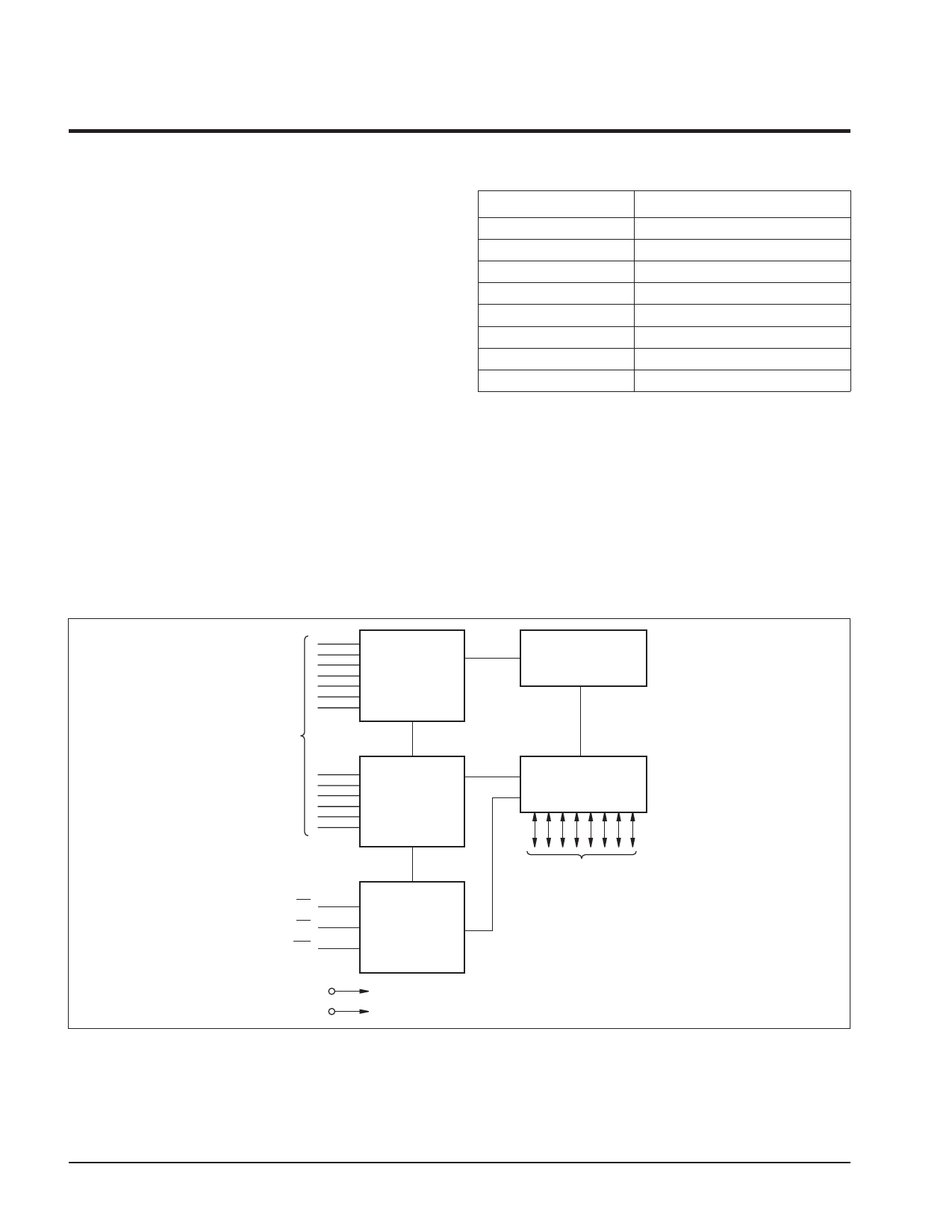
FUNCTIONAL DIAGRAM
A0–A12
ADDRESS
INPUTS
X BUFFERS
LATCHES AND
DECODER
Y BUFFERS
LATCHES AND
DECODER
65,536-BIT
E2PROM
ARRAY
I/O BUFFERS
AND LATCHES
Description
Address Inputs
Data Input/Output
Write Enable
Chip Enable
Output Enable
+5V
Ground
No Connect
3857 PGM T01
CE
OE
WE
VCC
VSS
CONTROL
LOGIC AND
TIMING
I/O0–I/O7
DATA INPUTS/OUTPUTS
3857 FHD F01
2
Share Link: 