Z53C80 查看數據表(PDF) - Zilog
零件编号
产品描述 (功能)
生产厂家
Z53C80 Datasheet PDF : 40 Pages
| |||
ZILOG
FUNCTIONAL DESCRIPTION
Z53C80 SCSI
General. The Small Computer System interface (SCSI)
device has a set of eight registers that are controlled by the
CPU. By reading and writing the appropriate registers, the
CPU may initiate any SCSI Bus activity or may sample and
assert any signal on the SCSI Bus. This allows the user to
implement all or any of the SCSI protocol in software. These
registers are read (written) by activating /CS with an
address on A2-A0 and then issuing a /RD (/WR) pulse. This
section describes the operation of the internal registers
(Table 1).
Table 1. Register Summary
Address
A2 A1 A0 R/W Register Name
0 0 0 R Current SCSI Data
0 0 0 W Output Data
0 0 1 R/W Initiator Command
0 1 0 R/W Mode
0 1 1 R/W Target Command
1 0 0 R Current SCSI Bus Status
1 0 0 W Select Enable
1 0 1 R Bus and Status
1 0 1 W Start DMA Send
1 1 0 R Input Data
1 1 0 W Start DMA Target Receive
1 1 1 R Reset Parity/Interrupt
1 1 1 W Start DMA Initiator Receive
Address: 0
(Read Only)
D7 D6 D5 D4 D3 D2 D1 D0
/DB0
/DB1
/DB2
/DB3
/DB4
/DB5
/DB6
/DB7
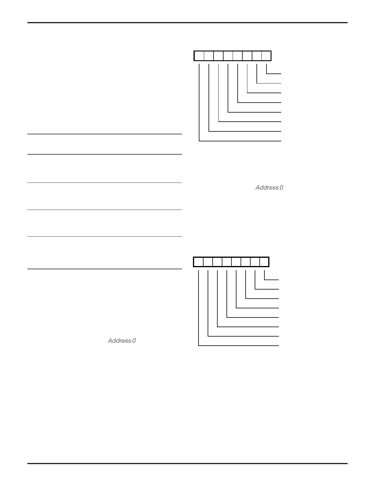
Figure 5. Current SCSI Data Register
Output Data Register. Address 0 (Write Only). The Output
Data Register (Figure 6) is a write-only register that is used
to send data to the SCSI Bus. This is accomplished by
either using a normal CPU write, or under DMA control, by
using /WR and /DACK. This register also asserts the
proper ID bits on the SCSI Bus during the Arbitration and
Selection phases.
Address: 0
(Write Only)
D7 D6 D5 D4 D3 D2 D1 D0
Data Registers. The data registers are used to transfer
SCSI commands, data, status, and message bytes between
the microprocessor Data Bus and the SCSI Bus. The SCSI
does not interpret any information that passes through the
data registers. The data registers consist of the transparent
Current SCSI Data Register, the Output Data Register, and
the Input Data Register.
Current SCSI Data Register. Address 0 (Read Only). The
Current SCSI Data Register (Figure 5) is a read-only
register which allows the microprocessor to read the active
SCSI Data Bus. This is accomplished by activating /CS
with an address on A2-A0 and issuing a /RD pulse. If parity
checking is enabled, the SCSI Bus parity is checked at the
beginning of the read cycle. This register is used during a
programmed I/O data read or during Arbitration to check
for higher priority arbitrating devices. Parity is not
guaranteed valid during Arbitration.
/DB0
/DB1
/DB2
/DB3
/DB4
/DB5
/DB6
/DB7
Figure 6. Output Data Register
PS97SCC0200
7
Share Link: 