2SJ610 查看數據表(PDF) - Toshiba
零件编号
产品描述 (功能)
生产厂家
2SJ610 Datasheet PDF : 6 Pages
| |||
2SJ610
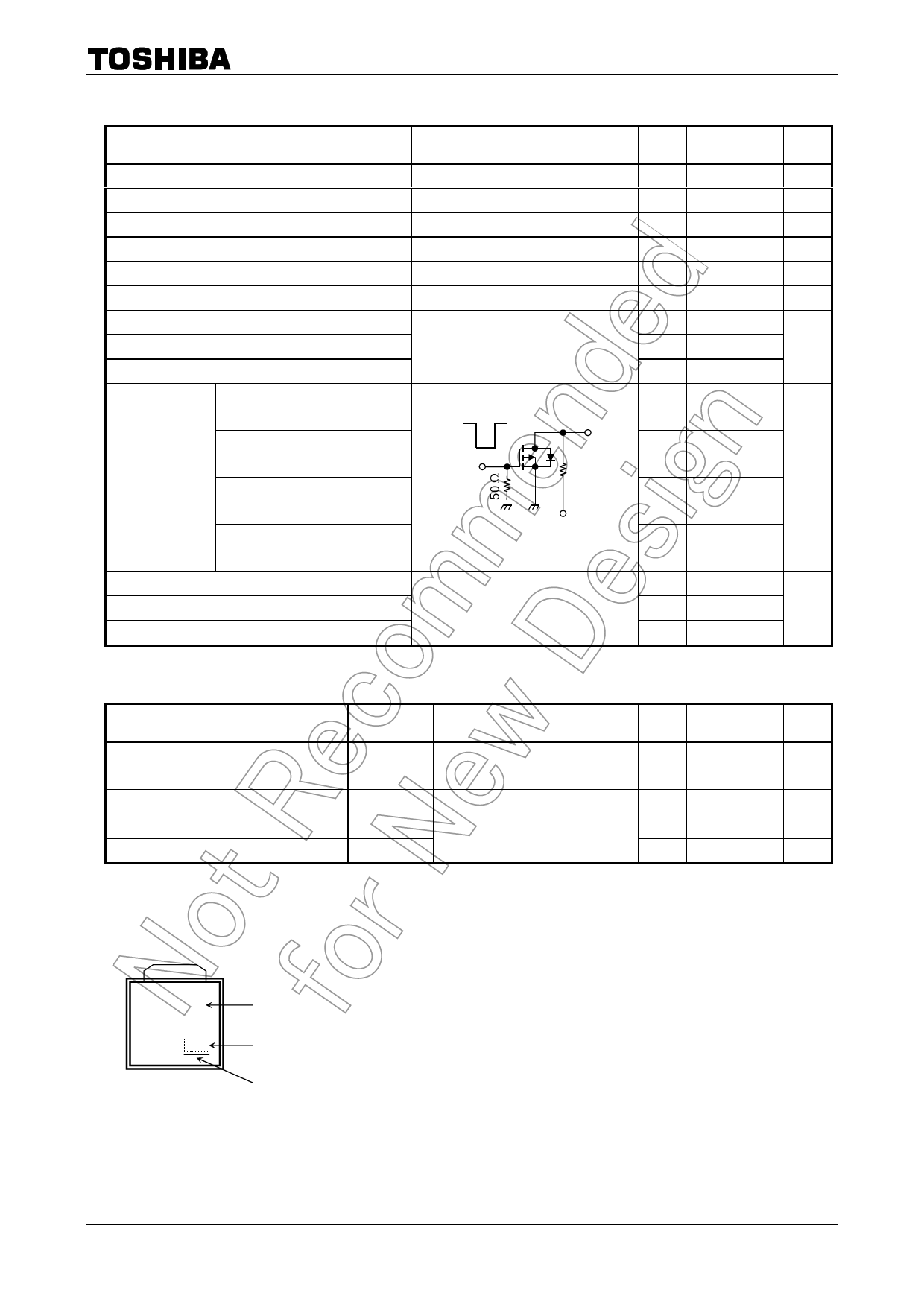
Electrical Characteristics (Ta = 25°C)
Characteristic
Gate leakage current
Drain cutoff current
Drain-source breakdown voltage
Gate threshold voltage
Drain-source ON-resistance
Forward transfer admittance
Input capacitance
Reverse transfer capacitance
Output capacitance
Rise time
Switching time
Turn-on time
Fall time
Turn-off time
Total gate charge
Gate-source charge
Gate-drain charge
Symbol
Test Condition
IGSS
IDSS
V (BR) DSS
Vth
RDS (ON)
⎪Yfs⎪
Ciss
Crss
Coss
VGS = ±16 V, VDS = 0 V
VDS = −250 V, VGS = 0 V
ID = −10 mA, VGS = 0 V
VDS = −10 V, ID = −1 mA
VGS = −10 V, ID = −1.0 A
VDS = −10 V, ID = −1.0 A
VDS = −10 V, VGS = 0 V, f = 1 MHz
Min Typ. Max Unit
⎯
⎯
±10
μA
⎯
⎯ −100 μA
−250 ⎯
⎯
V
−1.5
⎯
−3.5
V
⎯ 1.85 2.55 Ω
0.5 1.8
⎯
S
⎯ 381 ⎯
⎯
52
⎯
pF
⎯ 157 ⎯
tr
10 V
VGS
ton
0V
ID = 1.0 A VOUT
⎯
5
⎯
⎯
20
⎯
RL = 100 Ω
ns
tf
⎯
6
⎯
VDD ≈ 100 V
toff
Duty ≤ 1%, tw = 10 μs
⎯
36
⎯
Qg
VDD ≈ −200 V, VGS = −10 V,
Qgs
ID = −2.0 A
Qgd
⎯
24
⎯
⎯
11
⎯
nC
⎯
13
⎯
Source-Drain Ratings and Characteristics (Ta = 25°C)
Characteristic
Continuous drain reverse current (Note 1)
Pulse drain reverse current
(Note 1)
Forward voltage (diode)
Reverse recovery time
Reverse recovery charge
Symbol
IDR
IDRP
VDSF
trr
Qrr
Test Condition
⎯
⎯
IDR = −2.0 A, VGS = 0 V
IDR = −2.0 A, VGS = 0 V,
dIDR/dt = 100 A/μs
Min Typ. Max Unit
⎯
⎯
−2.0
A
⎯
⎯
−4.0
A
⎯
⎯
2.0
V
⎯
120
⎯
ns
⎯
540
⎯
nC
Marking
J610
Part No.
Lot No.
Note 4
Note 4 : A line under a Lot No. identifies the indication of product Labels
[[G]]/RoHS COMPATIBLE or [[G]]/RoHS [[Pb]]
Please contact your TOSHIBA sales representative for details as to
environmental matters such as the RoHS compatibility of Product.
The RoHS is Directive 2002/95/EC of the European Parliament and
of the Council of 27 January 2003 on the restriction of the use of certain
hazardous substances in electrical and electronic equipment.
2
2010-02-05
Share Link: 