X24164PI-2.7 查看數據表(PDF) - Xicor -> Intersil
零件编号
产品描述 (功能)
生产厂家
X24164PI-2.7 Datasheet PDF : 14 Pages
| |||
X24164
PIN DESCRIPTIONS
Serial Clock (SCL)
The SCL input is used to clock all data into and out of the
device.
Serial Data (SDA)
SDA is a bidirectional pin used to transfer data into and
out of the device. It is an open drain output and may be
wire-ORed with any number of open drain or open
collector outputs.
An open drain output requires the use of a pull-up
resistor. For selecting typical values, refer to the Pull-Up
Resistor selection graph at the end of this data sheet.
Device Select (S0, S1, S2)
The device select inputs (S0, S1, S2) are used to set the
second, third and fourth bits of the 8 bit slave address.
This allows up to eight X24164’s to share a common
bus. These inputs can be static or actively driven. If used
statically they must be tied to VSS or VCC as appropriate.
If actively driven, they must be driven to VSS or VCC. To
be compatible with the X24C16 these pins must all be
tied to VSS.
Pin Names
Symbol
S0–S2
SDA
SCL
TEST
VSS
VCC
Description
Device Select Inputs
Serial Data
Serial Clock
Hold at VSS
Ground
Supply Voltage
3846 PGM T01
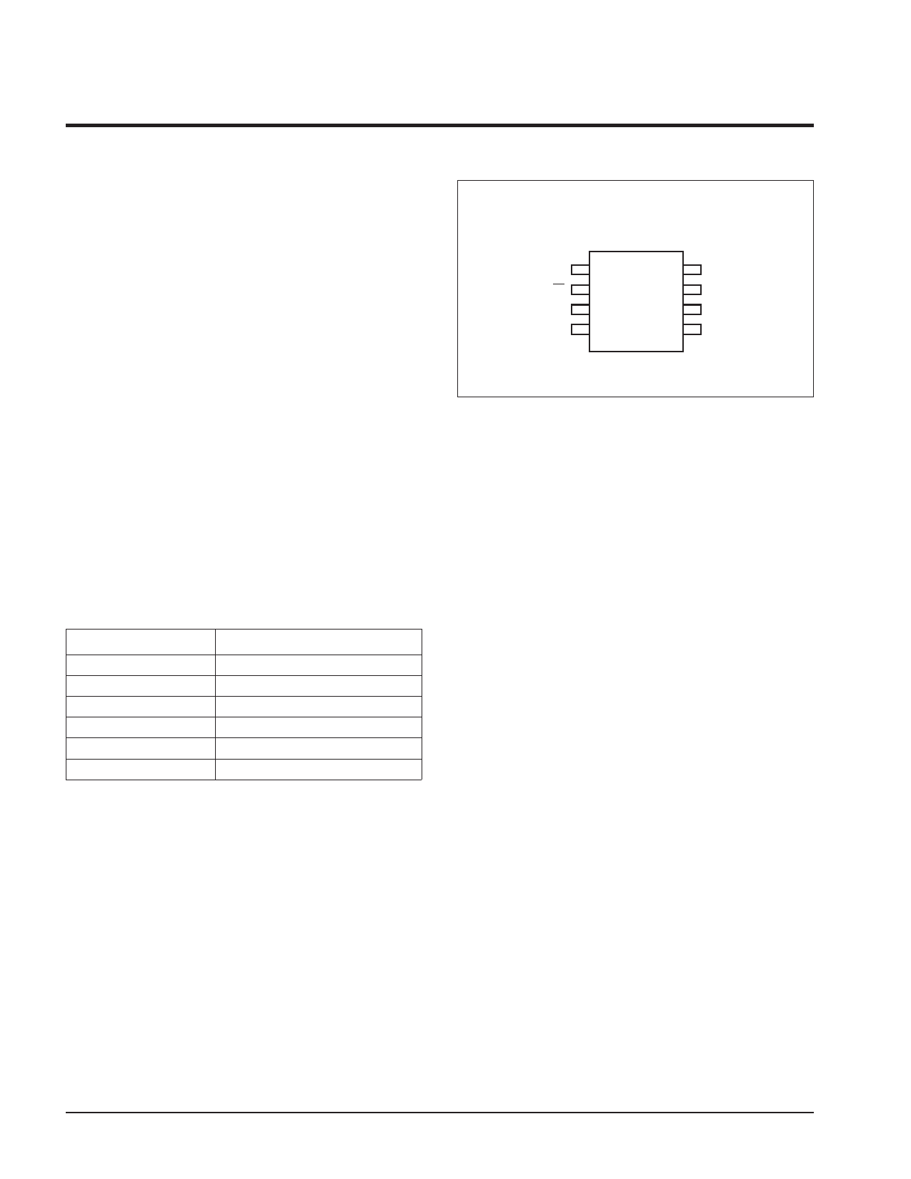
PIN CONFIGURATION
S0
S1
S2
VSS
DIP/SOIC
1
8
2
7
X24164
3
6
4
5
VCC
TEST
SCL
SDA
3846 FHD F02
2
Share Link: 