ISL8201M 查看數據表(PDF) - Intersil
零件编号
产品描述 (功能)
生产厂家
ISL8201M Datasheet PDF : 16 Pages
| |||
ISL8201M
Pin Functions
PGND (Pins 1, 2, 3, 4, 11)
Power ground pin for signal, input, and output return path.
PGND needs to connect to one (or more) ground plane(s)
immediately, which is recommended to minimize the effect of
switching noise, copper losses, and maximize heat dissipation.
PVCC (Pin 5)
This pin provides the bias supply for ISL8201M, as well as
the low-side MOSFET’s gate and high-side MOSFET’s gate.
If PVCC rises above 6.5V, an internal 5V regulator will
supply to the internal logics bias (but high-side and low-side
MOSFET gate will still be sourced by PVCC). Connect a well
decoupled +5V or +12V supply to this pin.
NC (Pins 6, 8, 15)
These pins have no function; do not connect.
ISET (Pin 7)
The ISET pin is the input for the overcurrent protection
(OCP) setting, which compares the rDS(ON) of the low-side
MOSFET to set the overcurrent threshold. The ISL8201M
has an initial protect overcurrent limit. It has an integrated
internal 3.57kΩ resistor (RSET-IN) between the ISET and
PGND pins, which can prevent significant overcurrent impact
to the module. One can also connect an additional resistor
RSET-EX between the ISET pin and the PGND pin in order to
reduce the current limit point by paralleling.
VIN (Pin 9)
Power input pin. Apply input voltage between the VIN pin
and PGND pin. It is recommended to place an input
decoupling capacitor directly between the VIN pin and the
PGND pin. The input capacitor should be placed as closely
as possible to the module.
PHASE (Pin 10)
The PHASE pin is the switching node between the high and
low side MOSFET. It also returns the current path for the
high side MOSFET driver and detects the low-side MOSFET
drain voltage for the overcurrent limits point.
VOUT (Pin 12)
Power output pin. Apply output load between this pin and the
PGND pin. It is recommended to place a high frequency
output decoupling capacitor directly between the VOUT pin
and the PGND pin. The output capacitor should be placed as
closely as possible to the module.
COMP/EN (Pin 13)
This is the multiplexed pin of the ISL8201M. During soft-start
and normal converter operation, this pin represents the
output of the error amplifier. Use COMP/EN in combination
with the FB pin to compensate for the voltage control
feedback loop of the converter. Pulling COMP/EN low
(VENDIS = 0.4V nominal) will disable (shut-down) the
controller, which causes the oscillator to stop, and the
high-side gate and low-side gate of the MOSFETs outputs to
be held low. The external pull-down device will initially need
to overcome a maximum of 5mA of COMP/EN output
current. However, once the controller is disabled, the
COMP/EN output will also be disabled, thus only a 20µA
current source will continue to draw current.
FB (Pin 14)
The FB pin is the output voltage adjustment of the ISL8201M.
It will regulate to 0.6V at the FB pin with respect to the PGND
pin. The ISL8201M has an integrated voltage dividing resistor.
This is a precision 9.76kΩ resistor (RFB-TI) between the VOUT
and FB pins. Different output voltages can be programmed
with additional resistors between FB to PGND.
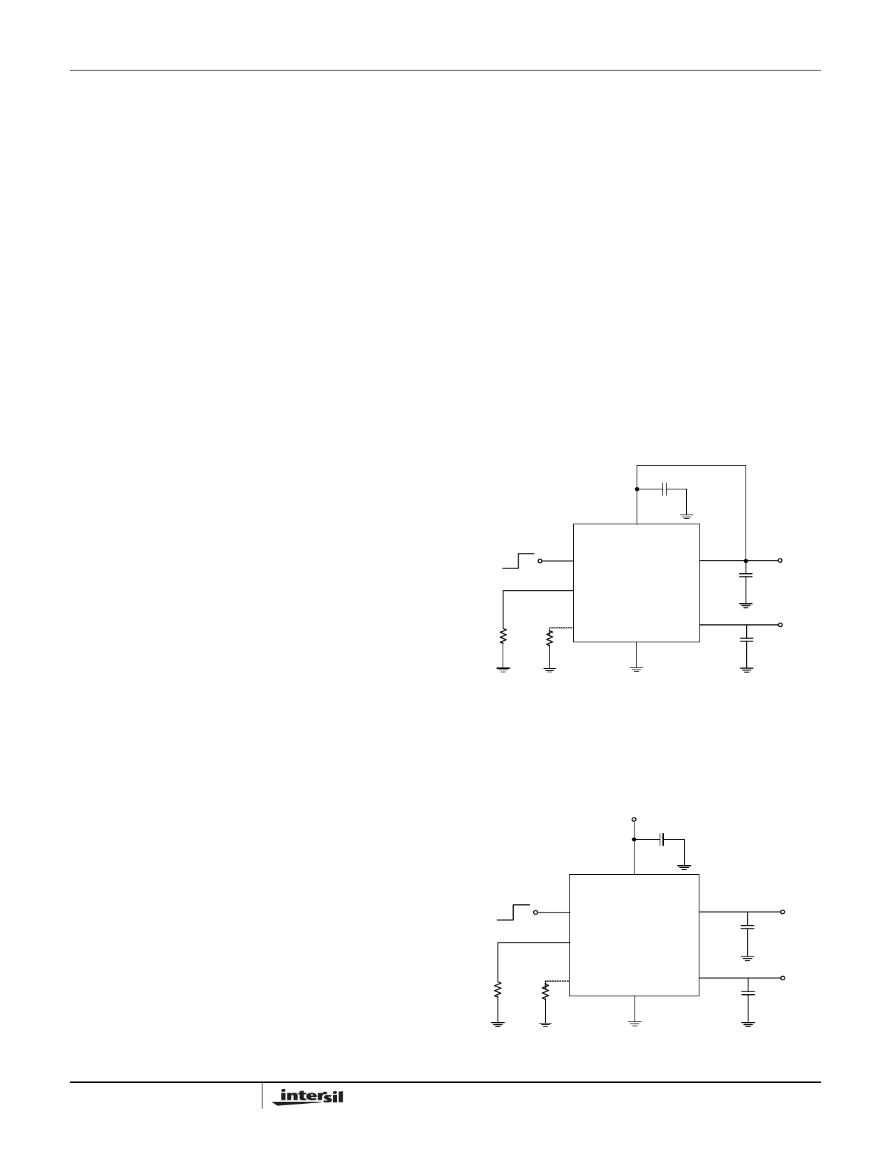
Reference Circuitry For General
Applications
Typical Application with Single Power Supply
Figure 11 shows the ISL8201M application schematic for
input voltage +5V or +12V. The PVCC pin can connect to the
input supply directly.
CPVCC
RFB RSET-EX
PVCC
COMP/EN
VIN
ISL8201M
FB
PHASE
ISET
VOUT
PGND
(+5V/+12V)
VIN
CIN
VOUT
COUT
FIGURE 11. TYPICAL APPLICATION SCHEMATIC
Typical Application with Separated Power Supply
Figure 12 shows the ISL8201M application schematic for
wide input voltages from +1V to +20V. The PVCC supply can
source +5V/+12V or +6.5V to 14.4V.
(+5V/+12V)
or
PVCC
(+6.5V to 14.4V) CPVCC
RFB RSET-EX
PVCC
COMP/EN
VIN
ISL8201M
FB
PHASE
ISET
VOUT
PGND
(+1V to +20V)
VIN
CIN
VOUT
COUT
FIGURE 12. WIDE INPUT VOLTAGE APPLICATION SCHEMATIC
7
FN6657.2
October 21, 2010
Share Link: 