LCMXO256E-3T100CES 查看數據表(PDF) - Lattice Semiconductor
零件编号
产品描述 (功能)
生产厂家
LCMXO256E-3T100CES Datasheet PDF : 95 Pages
| |||
Lattice Semiconductor
Architecture
MachXO Family Data Sheet
The ispLEVER design tool takes the output of the synthesis tool and places and routes the design. Generally, the
place and route tool is completely automatic, although an interactive routing editor is available to optimize the
design.
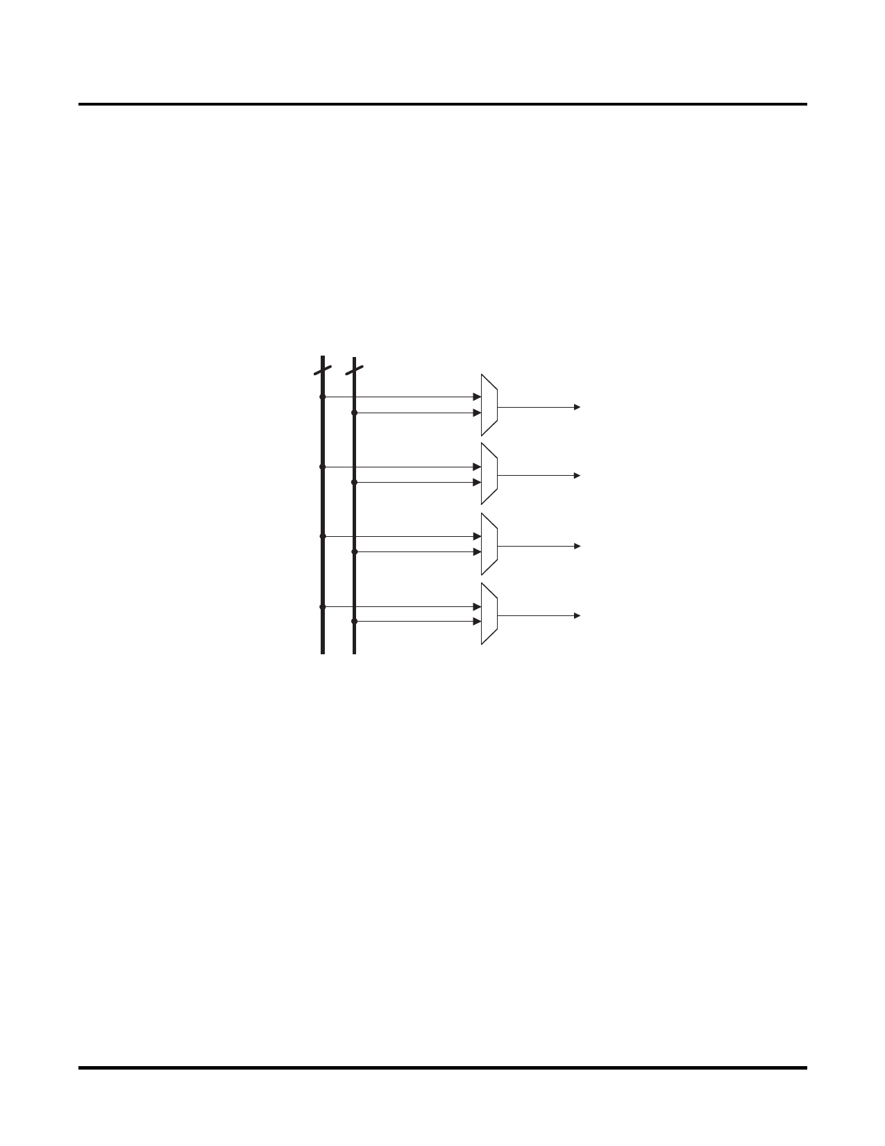
Clock/Control Distribution Network
The MachXO family of devices provides global signals that are available to all PFUs. These signals consist of four
primary clocks and four secondary clocks. Primary clock signals are generated from four 16:1 muxes as shown in
Figure 2-7 and Figure 2-8. The available clock sources for the MachXO256 and MachXO640 devices are four dual
function clock pins and 12 internal routing signals. The available clock sources for the MachXO1200 and
MachXO2280 devices are four dual function clock pins, up to nine internal routing signals and up to six PLL out-
puts.
Figure 2-7. Primary Clocks for MachXO256 and MachXO640 Devices
12
4
Primary Clock 0
16:1
Primary Clock 1
16:1
Primary Clock 2
16:1
Routing Clock
Pads
Primary Clock 3
16:1
2-7
Share Link: 