LCMXO2280E-3MN132CES 查看數據表(PDF) - Lattice Semiconductor
零件编号
产品描述 (功能)
生产厂家
LCMXO2280E-3MN132CES Datasheet PDF : 95 Pages
| |||
Lattice Semiconductor
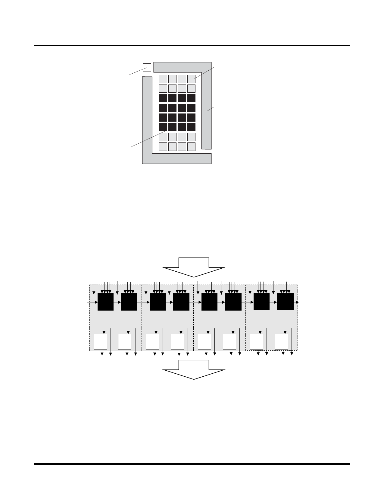
Figure 2-3. Top View of the MachXO256 Device
JTAG Port
Architecture
MachXO Family Data Sheet
Programmable Function
Units without RAM (PFFs)
PIOs Arranged
into sysIO Banks
Programmable
Function
Units with
RAM (PFUs)
PFU Blocks
The core of the MachXO devices consists of PFU and PFF blocks. The PFUs can be programmed to perform
Logic, Arithmetic, Distributed RAM, and Distributed ROM functions. PFF blocks can be programmed to perform
Logic, Arithmetic, and Distributed ROM functions. Except where necessary, the remainder of this data sheet will
use the term PFU to refer to both PFU and PFF blocks.
Each PFU block consists of four interconnected Slices, numbered 0-3 as shown in Figure 2-4. There are 53 inputs
and 25 outputs associated with each PFU block.
Figure 2-4. PFU Diagram
From
Routing
FCIN
LUT4 &
CARRY
LUT4 &
CARRY
Slice 0
LUT4 &
CARRY
LUT4 &
CARRY
Slice 1
LUT4 &
CARRY
LUT4 &
CARRY
Slice 2
LUT4 &
CARRY
LUT4 &
CARRY
FCO
Slice 3
D
FF/
Latch
D
FF/
Latch
D
FF/
Latch
D
FF/
Latch
D
FF/
Latch
D
FF/
Latch
D
FF/
Latch
D
FF/
Latch
To
Routing
Slice
Each Slice contains two LUT4 lookup tables feeding two registers (programmed to be in FF or Latch mode), and
some associated logic that allows the LUTs to be combined to perform functions such as LUT5, LUT6, LUT7, and
LUT8. There is control logic to perform set/reset functions (programmable as synchronous/asynchronous), clock
select, chip-select, and wider RAM/ROM functions. Figure 2-5 shows an overview of the internal logic of the Slice.
The registers in the Slice can be configured for positive/negative and edge/level clocks.
2-3
Share Link: 