M38515FC-SP 查看數據表(PDF) - Renesas Electronics
零件编号
产品描述 (功能)
生产厂家
M38515FC-SP Datasheet PDF : 91 Pages
| |||
3851 Group (Built-in 24 KB or more ROM)
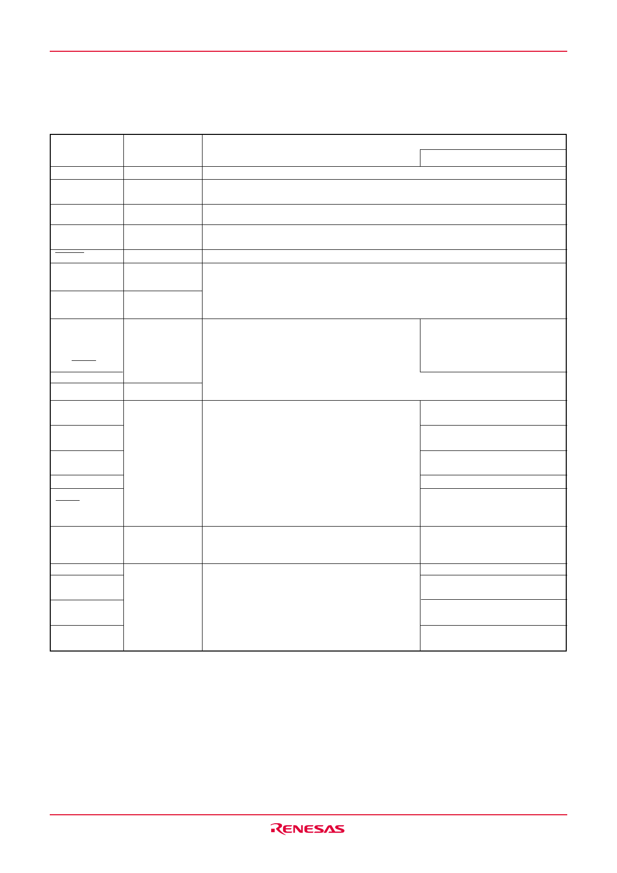
Table 1 Pin description
Pin
VCC, VSS
CNVSS
Name
Power source
CNVSS input
VREF
AVSS
RESET
XIN
Reference
voltage input
Analog power
source input
Reset input
Clock input
XOUT
Clock output
P00/SIN2
P01/SOUT2
P02/SCLK2
P03/SRDY2
P04–P07
P10–P17
P20/XCOUT
P21/XCIN
P22/SDA1
P23/SCL1
P24/SDA2/RxD
P25/SCL2/TxD
P26/SCLK1
P27/CNTR0/
SRDY1
I/O port P0
I/O port P1
I/O port P2
P30/AN0–
P34/AN4
I/O port P3
P40/CNTR1
P41/INT0
P42/INT1
P43/INT2/SCMP2
I/O port P4
P44/INT3/PWM
Functions
•Apply voltage of 2.7 V – 5.5 V to Vcc, and 0 V to Vss.
•This pin controls the operation mode of the chip.
•Normally connected to VSS.
•Reference voltage input pin for A-D converter.
Function except a port function
•Analog power source input pin for A-D converter.
•Connect to Vss.
•Reset input pin for active “L”.
•Input and output pins for the clock generating circuit.
•Connect a ceramic resonator or quartz-crystal oscillator between the XIN and XOUT pins to set
the oscillation frequency.
•When an external clock is used, connect the clock source to the XIN pin and leave the XOUT
pin open.
•8-bit CMOS I/O port.
•I/O direction register allows each pin to be individually
programmed as either input or output.
• Serial I/O2 function pin
•CMOS compatible input level.
•CMOS 3-state output structure.
•P10 to P17 (8 bits) are enabled to output large current
for LED drive.
•8-bit CMOS I/O port.
•I/O direction register allows each pin to be individually
programmed as either input or output.
•CMOS compatible input level.
• Sub-clock generating circuit I/O
pins (connect a resonator)
• I2C-BUS interface function pins
•P22 to P25 can be switched between CMOS compatible
input level or SMBUS input level in the I2C-BUS inter-
face function.
•P20, P21, P24 to P27: CMOS3-state output structure.
•P24, P25: N-channel open-drain structure in the I2C-
BUS interface function.
• I2C-BUS interface function pin/
Serial I/O1 function pins
• Serial I/O1 function pin
• Serial I/O1 function pin/Timer X
function pin
•P22, P23: N-channel open-drain structure.
•8-bit CMOS I/O port with the same function as port P0. • A-D converter input pin
•CMOS compatible input level.
•CMOS 3-state output structure.
•8-bit CMOS I/O port with the same function as port P0. • Timer Y function pin
•CMOS compatible input level.
• Interrupt input pins
•CMOS 3-state output structure.
• Interrupt input pin
• SCMP2 output pin
• Interrupt input pin
• PWM output pin
Rev.1.01 Oct 15, 2003 page 3 of 89
Share Link: 