MAX1717 查看數據表(PDF) - Maxim Integrated
零件编号
产品描述 (功能)
生产厂家
MAX1717 Datasheet PDF : 33 Pages
| |||
Dynamically Adjustable, Synchronous
Step-Down Controller for Notebook CPUs
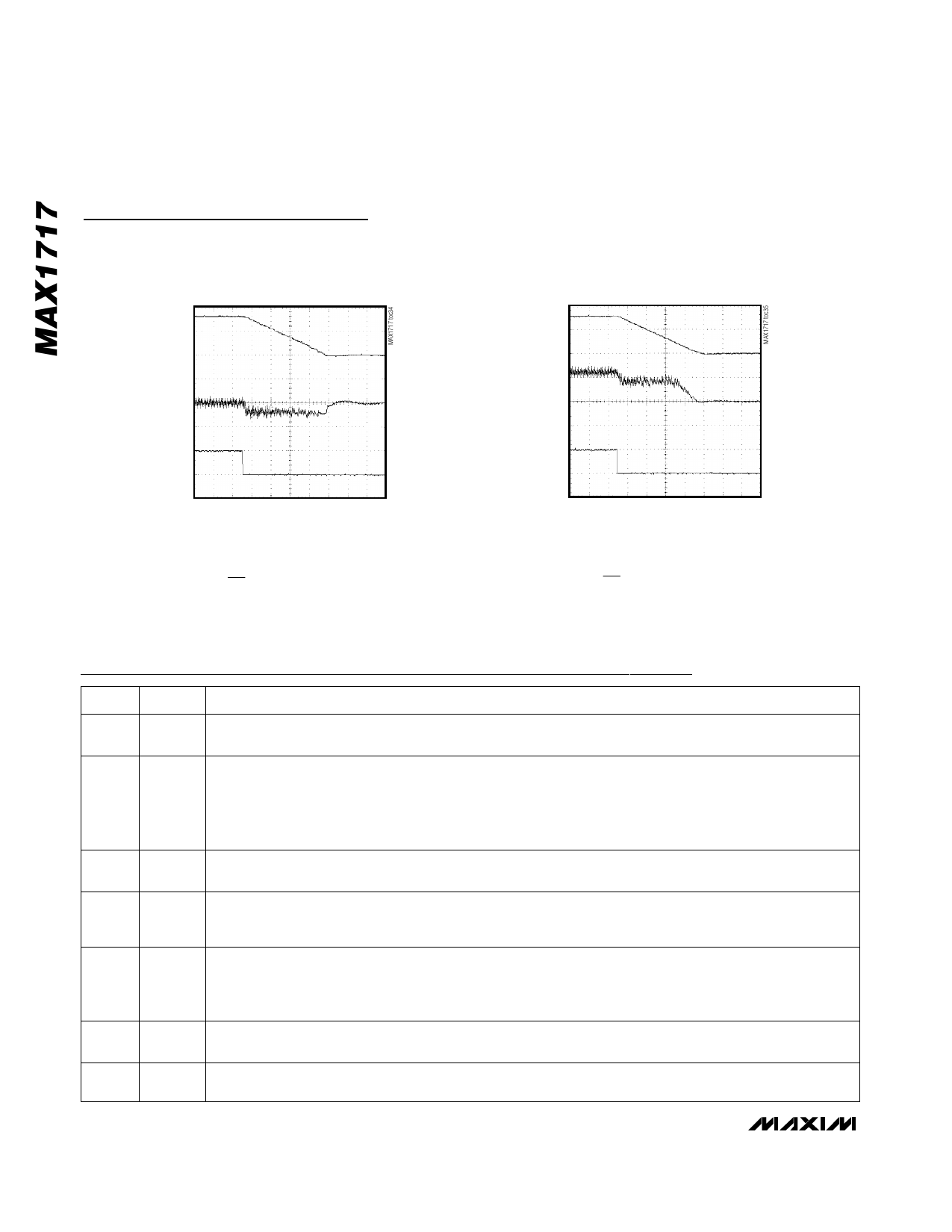
Typical Operating Characteristics (continued)
(Circuit of Figure 1, components of Table 1, V+ = +12V, VDD = VCC = SKP/SDN = +5V, VOUT = 1.6V, TA = +25°C, unless otherwise noted.)
SHUTDOWN WAVEFORM
SHUTDOWN WAVEFORM
A
A
B
B
C
100μs/div
300kHz VOLTAGE POSITIONED, CIRCUIT 2,
PWM MODE, NO LOAD
A = VOUT, 1V/div
B = INDUCTOR CURRENT, 10A/div
C = SKP/SDN, 5V/div
C
100μs/div
300kHz VOLTAGE POSITIONED, CIRCUIT 2,
PWM MODE, IOUT = 12A
A = VOUT, 1V/div
B = INDUCTOR CURRENT, 10A/div
C = SKP/SDN, 5V/div
Pin Description
PIN NAME
FUNCTION
1
V+
Battery Voltage Sense Connection. Connect V+ to input power source. V+ is used only for PWM one-shot
timing. DH on-time is inversely proportional to input voltage over a range of 2V to 28V.
Combined Shutdown and Skip-Mode Control. Drive SKP/SDN to GND for shutdown. Leave SKP/SDN open for
low-noise forced-PWM mode, or drive to VCC for normal pulse-skipping operation. Low-noise forced-PWM mode
2 SKP/SDN causes inductor current recirculation at light loads and suppresses pulse-skipping operation. SKP/SDN can also
be used to disable over/undervoltage protection circuits and clear the fault latch by forcing it to 12V < SKP/SDN
< 15V (with otherwise normal PFM/PWM operation). Do not connect SKP/SDN to > 15V.
3
TIME
Slew-Rate Adjustment Pin. Connect a resistor from TIME to GND to set the internal slew-rate clock. A 470kΩ
to 47kΩ resistor sets the clock from 38kHz to 380kHz, fSLEW = 150kHz x 120kΩ / RTIME.
Fast Feedback Input. Connect FB to the junction of the external inductor and output capacitor for nonvolt-
4
FB
age-positioned circuits (Figure 1). For voltage-positioned circuits, connect FB to the junction of the external
inductor and the positioning resistor (Figure 3).
Feedback Remote-Sense Input. For nonvoltage-positioned circuits, connect FBS to VOUT directly at the
5
FBS
load. FBS internally connects to the integrator that fine tunes the DC output voltage. For voltage-positioned
circuits, connect FBS directly to FB near the IC to disable the FBS remote-sense integrator amplifier. To dis-
able all three integrator amplifiers, connect FBS to VCC.
6
CC
Integrator Capacitor Connection. Connect a 100pF to 1000pF (470pF typ) capacitor from CC to GND to set
the integration time constant. CC can be left open if FBS is tied to VCC.
7
VCC
Analog Supply Voltage Input for PWM Core. Connect VCC to the system supply voltage (4.5V to 5.5V) with a
series 20Ω resistor. Bypass to GND with a 0.22µF (min) capacitor.
10 ______________________________________________________________________________________
Share Link: 