MAX1717 查看數據表(PDF) - Maxim Integrated
零件编号
产品描述 (功能)
生产厂家
MAX1717 Datasheet PDF : 33 Pages
| |||
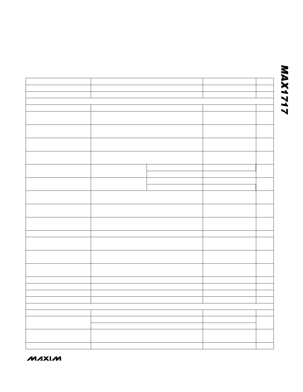
Dynamically Adjustable, Synchronous
Step-Down Controller for Notebook CPUs
ELECTRICAL CHARACTERISTICS (continued)
(Circuit of Figure 1, V+ = +15V, VCC = VDD = SKP/SDN = +5V, VOUT = 1.6V, TA = 0°C to +85°C, unless otherwise noted.)
PARAMETER
Reference Load Regulation
REF Sink Current
FAULT PROTECTION
Overvoltage Trip Threshold
IREF = 0 to 50µA
REF in regulation
CONDITIONS
Measured at FB
MIN TYP MAX
0.01
10
2.20 2.25 2.30
Overvoltage Fault Propagation
Delay
FB forced 2% above trip threshold
10
UNITS
V
µA
V
µs
Output Undervoltage Fault
Protection Threshold
With respect to unloaded output voltage
65
70
75
%
Output Undervoltage Fault
Propagation Delay
FB forced 2% below trip threshold
10
µs
Output Undervoltage Fault
Blanking Time
Current-Limit Threshold
(Positive, Default)
Current-Limit Threshold
(Positive, Adjustable)
Current-Limit Threshold
(Negative)
From SKP/SDN signal going high, clock speed set by RTIME
256
clks
GND - LX, ILIM = VCC
GND - LX
TA = +25°C to +85°C
TA = 0°C to +85°C
ILIM = 0.5V
ILIM = REF (2V)
90
100
110
mV
85
115
35
50
65
mV
165
200
230
LX - GND, ILIM = VCC
-140 -110
-80
mV
Current-Limit Threshold
(Zero Crossing)
GND - LX
4
mV
Current-Limit Default
Switchover Threshold
Thermal Shutdown Threshold
VCC Undervoltage Lockout
Threshold
Hysteresis = 10°C
Rising edge, hysteresis = 20mV, PWM disabled below
this level
3 VCC - 1 VCC - 0.4 V
150
°C
4.1
4.4
V
VGATE Lower Trip Threshold
Measured at FB with respect to unloaded output voltage,
rising edge, hysteresis = 1%
-8
-6.5
-5
%
VGATE Upper Trip Threshold
Measured at FB with respect to unloaded output voltage,
rising edge, hysteresis = 1%
+10
+12
+14
%
VGATE Propagation Delay
VGATE Transition Delay
VGATE Output Low Voltage
VGATE Leakage Current
GATE DRIVERS
DH Gate Driver On-Resistance
DL Gate Driver On-Resistance
FB forced 2% outside VGATE trip threshold
After X = Y, clock speed set by RTIME
ISINK = 1mA
High state, forced to 5.5V
BST - LX forced to 5V
DL, high state (pullup)
DL, low state (pulldown)
10
µs
1
clk
0.4
V
1
µA
1.0
3.5
Ω
1.0
3.5
Ω
0.4
1.0
DH Gate-Driver Source/Sink
Current
DH forced to 2.5V, BST - LX forced to 5V
1.3
A
DL Gate-Driver Sink Current
DL forced to 2.5V
4
A
_______________________________________________________________________________________ 3
Share Link: 