MCP602 查看數據表(PDF) - Microchip Technology
零件编号
产品描述 (功能)
生产厂家
MCP602 Datasheet PDF : 34 Pages
| |||
MCP601/1R/2/3/4
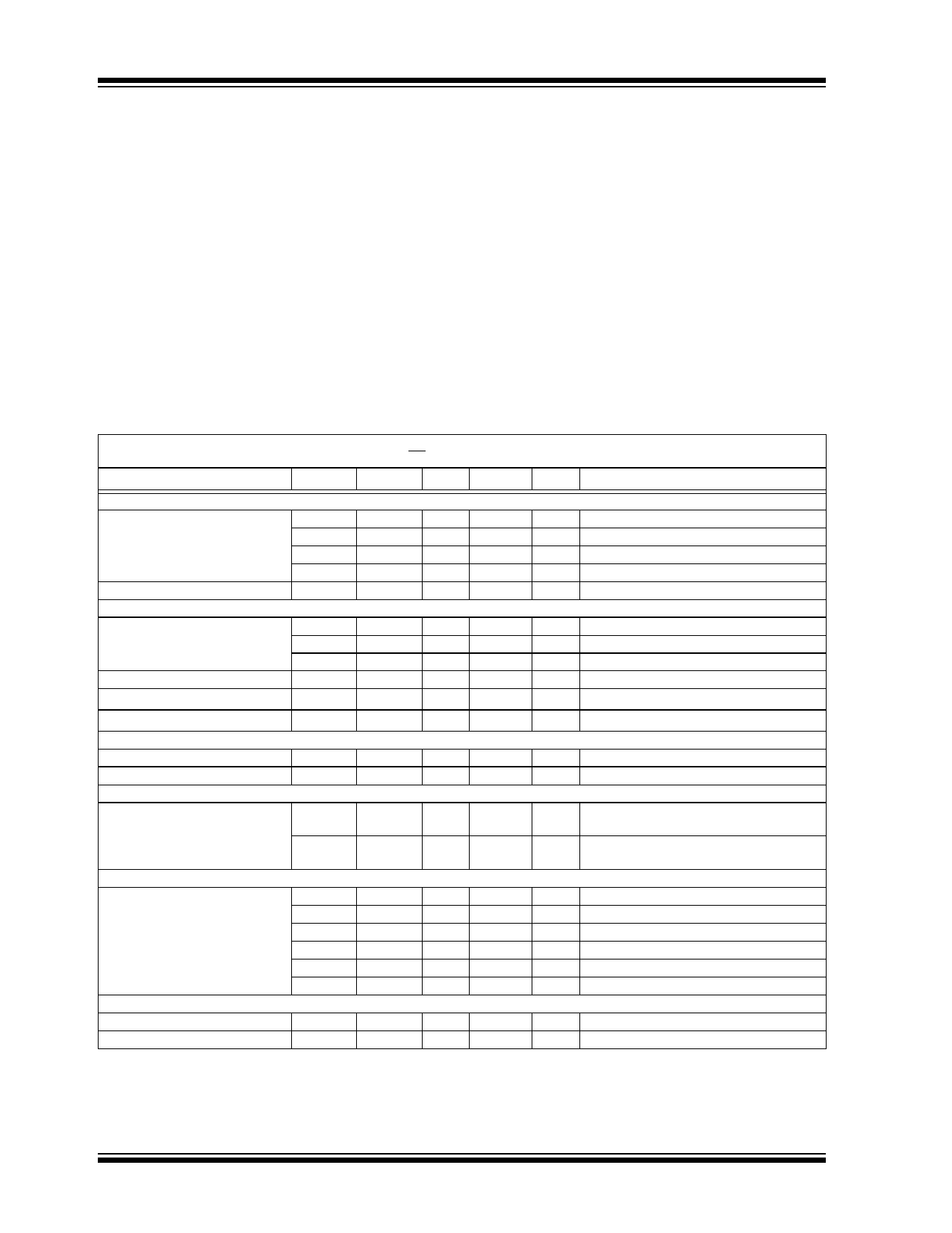
1.0 ELECTRICAL
CHARACTERISTICS
Absolute Maximum Ratings †
VDD – VSS ........................................................................7.0V
Current at Input Pins .....................................................±2 mA
Analog Inputs (VIN+, VIN–) †† ........ VSS – 1.0V to VDD + 1.0V
All Other Inputs and Outputs ......... VSS – 0.3V to VDD + 0.3V
Difference Input Voltage ...................................... |VDD – VSS|
Output Short Circuit Current .................................Continuous
Current at Output and Supply Pins ............................±30 mA
Storage Temperature....................................–65°C to +150°C
Maximum Junction Temperature (TJ) ......................... .+150°C
ESD Protection On All Pins (HBM; MM) .............. ≥ 3 kV; 200V
† Notice: Stresses above those listed under “Absolute
Maximum Ratings” may cause permanent damage to the
device. This is a stress rating only and functional operation of
the device at those or any other conditions above those
indicated in the operational listings of this specification is not
implied. Exposure to maximum rating conditions for extended
periods may affect device reliability.
†† See Section 4.1.2 “Input Voltage and Current Limits”.
DC CHARACTERISTICS
Electrical Specifications: Unless otherwise specified, TA = +25°C, VDD = +2.7V to +5.5V, VSS = GND, VCM = VDD/2,
VOUT ≈ VDD/2, VL = VDD/2, and RL = 100 kΩ to VL, and CS is tied low. (Refer to Figure 1-2 and Figure 1-3).
Parameters
Sym
Min
Typ
Max Units
Conditions
Input Offset
Input Offset Voltage
Industrial Temperature
Extended Temperature
Input Offset Temperature Drift
Power Supply Rejection
VOS
-2
VOS
-3
VOS
-4.5
ΔVOS/ΔTA
—
PSRR
80
Input Current and Impedance
±0.7
+2
mV
±1
+3
mV TA = -40°C to +85°C (Note 1)
±1
+4.5
mV TA = -40°C to +125°C (Note 1)
±2.5
—
µV/°C TA = -40°C to +125°C
88
—
dB VDD = 2.7V to 5.5V
Input Bias Current
IB
Industrial Temperature
IB
Extended Temperature
IB
Input Offset Current
IOS
Common Mode Input Impedance
ZCM
—
1
—
pA
—
20
60
pA TA = +85°C (Note 1)
—
450 5000
pA TA = +125°C (Note 1)
—
±1
—
pA
—
1013||6
—
Ω||pF
Differential Input Impedance
ZDIFF
—
1013||3
—
Ω||pF
Common Mode
Common Mode Input Range
Common Mode Rejection Ratio
Open-loop Gain
VCMR VSS – 0.3 — VDD – 1.2 V
CMRR
75
90
—
dB VDD = 5.0V, VCM = -0.3V to 3.8V
DC Open-loop Gain (large signal) AOL
AOL
Output
100
115
—
dB RL = 25 kΩ to VL,
VOUT = 0.1V to VDD – 0.1V
95
110
—
dB RL = 5 kΩ to VL,
VOUT = 0.1V to VDD – 0.1V
Maximum Output Voltage Swing
Linear Output Voltage Swing
Output Short Circuit Current
Power Supply
VOL, VOH VSS + 15 — VDD – 20 mV RL = 25 kΩ to VL, Output overdrive = 0.5V
VOL, VOH VSS + 45 — VDD – 60 mV RL = 5 kΩ to VL, Output overdrive = 0.5V
VOUT VSS + 100 — VDD – 100 mV RL = 25 kΩ to VL, AOL ≥ 100 dB
VOUT VSS + 100 — VDD – 100 mV RL = 5 kΩ to VL, AOL ≥ 95 dB
ISC
—
±22
—
mA VDD = 5.5V
ISC
—
±12
—
mA VDD = 2.7V
Supply Voltage
VDD
2.7
—
6.0
V (Note 2)
Quiescent Current per Amplifier
IQ
—
230
325
µA IO = 0
Note 1: These specifications are not tested in either the SOT-23 or TSSOP packages with date codes older than YYWW = 0408.
In these cases, the minimum and maximum values are by design and characterization only.
2: All parts with date codes November 2007 and later have been screened to ensure operation at VDD=6.0V. However, the
other minimum and maximum specifications are measured at 1.4V and/or 5.5V.
DS21314G-page 2
© 2007 Microchip Technology Inc.
Share Link: 