STV6412ADT 查看數據表(PDF) - STMicroelectronics
零件编号
产品描述 (功能)
生产厂家
STV6412ADT Datasheet PDF : 31 Pages
| |||
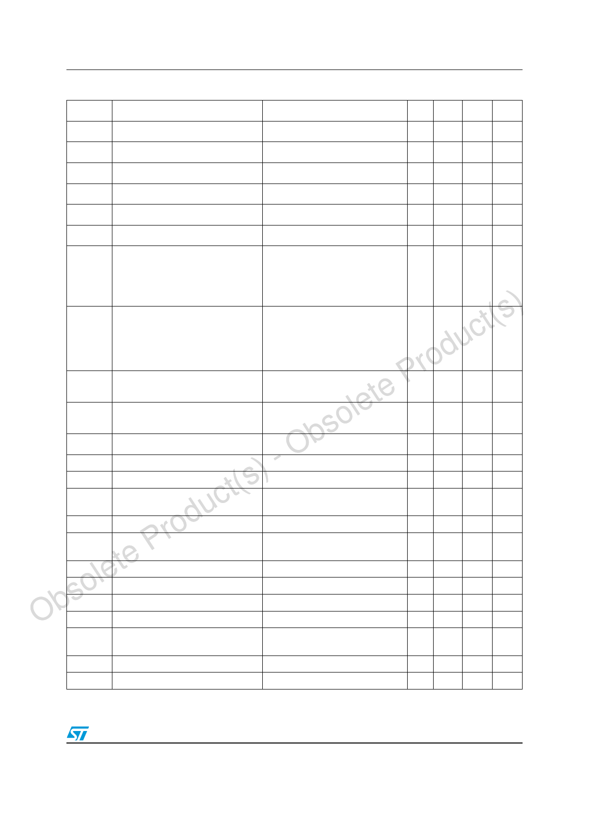
STV6412A
Electrical characteristics
Table 6.
Symbol
Video section characteristics
Parameter
Test condition
Min. Typ. Max. Unit
VDCIN DC input level
Bottom synch pulse
2
V
ICLAMP Clamping current
at VDCIN -400 mV
12
mA
ILEAK Input leakage current
VIN = VDCIN +1 V
1 10 µA
CIN Input capacitance
2
pF
VIN Max input signal
VCC = 5 V
1.5
VPP
DYN Dynamic output signal
VCC = 5 V
3
VPP
BW Bandwidth at -3 dB
Y/CVBS
VIN = 1 VPP
12 15
MHz
RGB
VIN = 1 VPP
12 15
MHz
Y/C mixer (on VOUT-RF) VIN = 1 VPP, VINC = muted
duct(s) Flatness
Spread of gain in video band
(15 kHz - 5 MHz)
Y/CVBS
VIN = 1 VPP
RGB
VIN = 1 VPP
Y/C Mixer (on VOUT-RF) VIN = 1 VPP, VINC = muted
Pro CTi
Crosstalk isolation between input
channel
VIN = 1 VPP at f = 4.43 MHz,
on one point
olete CTo
Crosstalk isolation between output VIN = 1 VPP at f = 4.43 MHz,
channel
on one point, RLOAD = 150Ω
bs ROUT Output resistance
- O GRGB Gain at RGB outputs
) GRGBM Gain matching between R, G, B
ct(s GRGBSTE Step of gain
P
du GYCVBS Gain on Y,/CVBS channels
Pro GYCVBSM
Gain matching between Y, CVBS
inputs
te DCOUT DC output voltage
le DCOUT RF RF output voltage
soDPHI Differential phase
Ob DG Differential gain
VIN = 1 Vpp, gain set to 6 dB
VIN = 1 VPP, gain set to 6 dB
3 dB to 6 dB
VIN = 1 VPP
VIN = 1 VPP
Bottom sync pulse
Bottom sync pulse
VIN = 1 VPP at f = 4.43 MHz
VIN = 1 VPP at f = 4.43 MHz
8 10
MHz
+/-0.5 dB
+/-0.5 dB
+/-1.5 dB
60
dB
50
dB
5 10 Ω
5.5
6
-0.3
0
6.5
dB
0.3
dB
0.75
1
1.25
dB
5.5
6
6.5
dB
-0.5
0
0.5
dB
0.6
V
1
V
1
5 ° deg.
1
5
%
Mute Mute suppression
VIN = 1 VPP at f = 5 MHz on one
point
-55
dB
LNL Luminance non-linerarity
0.3 3
%
VSN Video S/N ratio
Refer to Note 1
65
dB
Note: 1 S/N = 20 log (VOUT Black to White = 0.7 VPP / VNoise (mVRMS) weighted CCIR 567).
Doc ID 9754 Rev 2
11/31
Share Link: 