TC7650 查看數據表(PDF) - TelCom Semiconductor, Inc
零件编号
产品描述 (功能)
生产厂家
TC7650 Datasheet PDF : 7 Pages
| |||
CHOPPER-STABILIZED
OPERATIONAL AMPLIFIER
TC7650
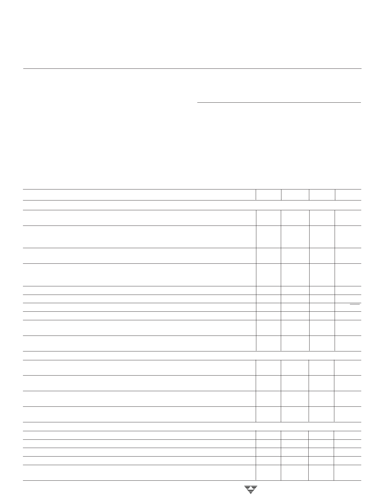
ABSOLUTE MAXIMUM RATINGS*
Total Supply Voltage (VDD to VSS) .............................. 18V
Input Voltage ........................ (VDD + 0.3V) to (VSS – 0.3V)
Storage Temperature Range ................ – 65°C to +150°C
Lead Temperature (Soldering, 10 sec) ................... 300°C
Voltage on Oscillator Control Pins ................... VDD to VSS
Output Short Circuit Duration ............................. Indefinite
Current Into Any Pin ................................................. 10mA
While Operating (Note 3) .................................. 100µA
Operating Temperature Range
C Device ................................................ 0°C to +70°C
Package Power Dissipation (TA ≤ 70°C)
8-Pin Plastic DIP ............................................. 730mW
14-Pin Plastic DIP ...........................................800mW
*Static-sensitive device. Unused devices must be stored in conductive
material. Protect devices from static discharge and static fields. Stresses
above those listed under Absolute Maximum Ratings may cause perma-
nent damage to the device. These are stress ratings only and functional
operation of the device at these or any other conditions above those
indicated in the operational sections of the specifications is not implied.
Exposure to Absolute Maximum Rating Conditions for extended periods
may affect device reliability.
ELECTRICAL CHARACTERISTICS: VDD = +5V, VSS = –5V, CA = CB = 0.1µF, TA = 25°C, unless otherwise
indicated.
Symbol
Parameter
Test Conditions
Min Typ Max Units
Input
VOS
∆VOS/∆T
IBIAS
IOS
eNP-P
IN
RIN
CMVR
CMRR
Output
A
VOUT
Dynamic
BW
SR
tR
fCH
Input Offset Voltage
Input Offset Voltage
Average Temperature
Coefficient
Offset Voltage vs. Time
Input Bias Current
Input Offset Current
Input Noise Voltage
Input Noise Current
Input Resistance
Common-Mode
Voltage Range
Common-Mode
Rejection Ratio
TA = +25°C
Over Operating Temp Range
Operating Temperature Range
TA = +25°C
0°C ≤ TA ≤ +70°C
–25°C ≤ TA ≤ +85°C
RS = 100Ω, 0 to 10Hz
f = 10 Hz
CMVR = –5V to +1.5V
Large Signal Voltage
Gain
Output Voltage Swing (Note 2)
Clamp ON Current
Clamp OFF Current
RL = 10kΩ
RL = 10kΩ
RL = 100kΩ
RL = 100kΩ
(Note 1)
– 4V < VOUT < +4V
(Note 1)
Unity-Gain Bandwidth
Slew Rate
Rise Time
Overshoot
Internal Chopping
Frequency
Unity Gain (+1)
CL = 50 pF, RL = 10kΩ
Pins 12–14 Open (DIP)
—
±0.7
±5
—
—
± 1.0
—
µV
—
0.01
0.05 µV/°C
—
100
—
nV/
month
—
1.5
10
pA
—
35
150
pA
—
100
400
pA
—
0.5
—
pA
—
2
—
µVP-P
—
0.01
— pA/√Hz
—
1012
Ω
–5
– 5.2 +1.6
V
to +2
120
130
—
dB
120
130
—
dB
±4.7 ±4.85
—
V
—
±4.95
—
V
25
70
200
µA
—
1
—
pA
—
2.0
—
MHz
—
2.5
— V/µsec
—
0.2
—
µsec
—
20
—
%
120
200
375
Hz
3-274
TELCOM SEMICONDUCTOR, INC.
Share Link: 