TC7650 查看數據表(PDF) - TelCom Semiconductor, Inc
零件编号
产品描述 (功能)
生产厂家
TC7650 Datasheet PDF : 7 Pages
| |||
CHOPPER-STABILIZED
OPERATIONAL AMPLIFIER
1
TC7650
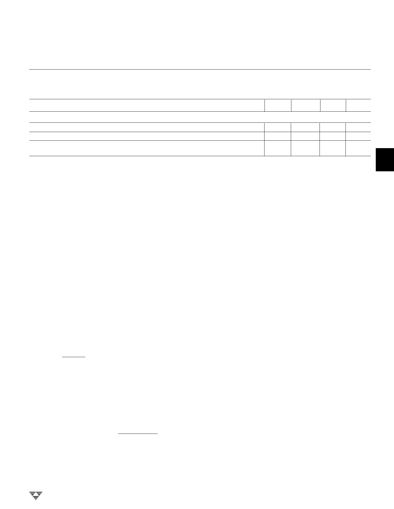
ELECTRICAL CHARACTERISTICS: VDD = +5V, VSS = – 5V, CA = CB = 0.1µF, TA = 25°C, unless otherwise
Symbol
Parameter
specified.
Test Conditions
2
Min Typ Max Units
Supply
VDD, VSS
Operating Supply Range
4.5
—
16
V
IS
Supply Current
No Load
—
2
3.5
mA
PSRR
Power Supply
Rejection Ratio
VS = ±3V to ±8V
120
130
NOTES: 1. See "Output Clamp" discussion.
2. Output clamp not connected. See typical characteristics curves for output swing versus clamp current characteristics.
3. Limiting input current to 100µA is recommended to avoid latch-up problems.
dB
3
Theory of Operation
As desired, the device offset voltages are reduced by
Figure 1 shows the major elements of the TC7650. the high open-loop gain of the nulling amplifier.
There are two amplifiers (the main amplifier and the nulling
amplifier), and both have offset-null capability. The main Output Stage/Loading
amplifier is connected full-time from the input to the output.
The nulling amplifier, under the control of the chopping
frequency oscillator and clock circuit, alternately nulls itself
and the main amplifier. Two external capacitors provide the
required storage of the nulling potentials and the necessary
nulling-loop time constants. The nulling arrangement oper-
ates over the full common-mode and power-supply ranges,
and is also independent of the output level, thus giving
exceptionally high CMRR, PSRR, and AVOL.
Careful balancing of the input switches minimizes chop-
per frequency charge injection at the input terminals, and the
feed-forward-type injection into the compensation capacitor
that can cause output spikes in this type of circuit.
The circuit's offset voltage compensation is easily shown.
With the nulling inputs shorted, a voltage almost identical to
4 The output circuit is a high-impedance stage (approxi-
mately 18kΩ). With loads less than this, the chopper ampli-
fier behaves in some ways like a transconductance amplifier
whose open-loop gain is proportional to load resistance. For
example, the open-loop gain will be 17dB lower with a 1kΩ
load than with a 10kΩ load. If the amplifier is used strictly for
DC, the lower gain is of little consequence, since the DC gain
is typically greater than 120dB, even with a 1kΩ load. In
5 wideband applications, the best frequency response will be
achieved with a load resistor of 10kΩ or higher. This results
in a smooth 6 dB/octave response from 0.1Hz to 2 MHz, with
phase shifts of less than 10° in the transition region, where
the main amplifier takes over from the null amplifier. The
clock frequency sets the transition region.
the nulling amplifier offset voltage is stored on CA. The
effective offset voltage at the null amplifier input is:
VOSE =
1
AN + 1
VOSN
(1)
After the nulling amplifier is zeroed, the main amplifier is
zeroed; the A switches open and B switches close.
The output voltage equation is:
Intermodulation
6 Previous chopper-stabilized amplifiers have suffered
from intermodulation effects between the chopper frequency
and input signals. These arise because the finite AC gain of
the amplifier results in a small AC signal at the input. This is
seen by the zeroing circuit as an error signal, which is
chopped and fed back, thus injecting sum and difference
frequencies, and causing disturbances to the gain and
VOUT = AM [VOSM + (V+ – V–) + AN(V+– V–) + AN VOSE](2)
Substituting (1) → (2) and assuming AN >>1:
[ ] VOUT = AM AN
(V+ – V–) + VOSM + VOSN
AN
(3)
phase versus frequency characteristics near the chopping
7 frequency. These effects are substantially reduced in the
TC7650 by feeding the nulling circuit with a dynamic current
corresponding to the compensation capacitor current in
such a way as to cancel that portion of the input signal due
to a finite AC gain. The intermodulation and gain/phase
disturbances are held to very low values, and can generally
be ignored.
8
TELCOM SEMICONDUCTOR, INC.
3-275
Share Link: 