TC7650 查看數據表(PDF) - TelCom Semiconductor, Inc
零件编号
产品描述 (功能)
生产厂家
TC7650 Datasheet PDF : 7 Pages
| |||
CHOPPER-STABILIZED
OPERATIONAL AMPLIFIER
TC7650
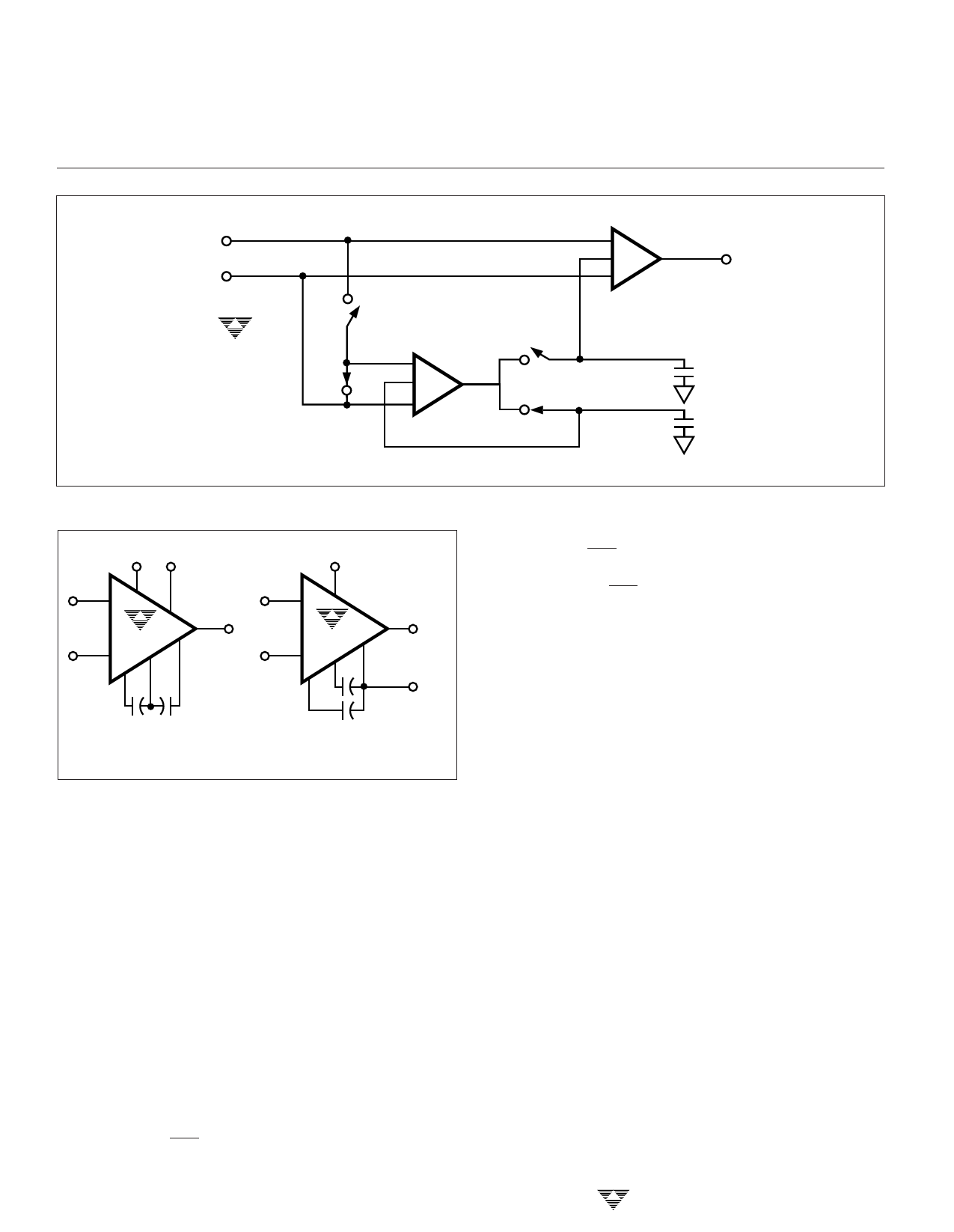
V+
ANALOG INPUT
V–
B
MAIN
+ AMPLIFIER
NULL
–
GAIN = AM
VOUT
TC7650
+
B
A
NULL
–
A
CB
NULL
CA
AMPLIFIER
GAIN = AN , OFFSET = VOSN
Figure 1. TC7650 Contains a Nulling and Main Amplifier. Offset Correction Voltages Are Stored on Two External Capacitors.
VDD VSS
VDD
4 – 11
7
10
5
TC7650
+
1
8
2
2–
7
6
3
TC7650
+
4
8 CB
1
VSS
CA CB
CA
14-PIN PACKAGE
8-PIN PACKAGE
Figure 2. Nulling Capacitor Connection
Nulling Capacitor Connection
The offset voltage correction capacitors are connected
to CA and CB. The common capacitor connection is made to
VSS (pin 4) on the 8-pin packages and to capacitor return
(CR, pin 8) on the 14-pin packages. The common connec-
tion should be made through a separate PC trace or wire to
avoid voltage drops. The capacitors outside foil, if possible,
should be connected to CR or VSS.
Clock Operation
The internal oscillator is set for a 200Hz nominal chop-
ping frequency on both the 8- and 14-pin DIPs. With the
14-pin DIP TC7650, the 200Hz internal chopping frequency
is available at the internal clock output (pin 12). A 400Hz
nominal signal will be present at the external clock input pin
(pin 13) with INT/EXT high or open. This is the internal clock
signal before a divide-by-two operation.
3-276
The 14-pin DIP device can be driven by an external
clock. The INT/EXT input (pin 14) has an internal pull-up and
may be left open for internal clock operation. If an external
clock is used, INT/EXT must be tied to VSS (pin 7) to disable
the internal clock. The external clock signal is applied to the
external clock input (pin 13).
The external clock amplitude should swing between
VDD and ground for power supplies up to ±6V and between
V+ and V+ – 6V for higher supply voltages.
At low frequencies the external clock duty cycle is not
critical, since an internal divide-by-two gives the desired
50% switching duty cycle. The offset storage correction
capacitors are charged only when the external clock input is
high. A 50% to 80% external clock positive duty cycle is
desired for frequencies above 500Hz to guarantee tran-
sients settle before the internal switches open.
The external clock input can also be used as a strobe
input. If a strobe signal is connected at the external clock
input so that it is LOW during the time an overload signal is
applied, neither capacitor will be charged. The leakage
currents at the capacitors pins are very low. At 25°C a typical
TC7650 will drift less than 10µV/sec.
Output Clamp
Chopper-stabilized systems can show long recovery
times from overloads. If the output is driven to either supply
rail, output saturation occurs. The inputs are no longer held
at a "virtual ground." The VOS null circuit treats the differen-
tial signal as an offset and tries to correct it by charging the
external capacitors. The nulling circuit also saturates. Once
the input signal returns to normal, the response time is
lengthened by the long recovery time of the nulling amplifier
and external capacitors.
Through an external clamp connection, the TC7650
TELCOM SEMICONDUCTOR, INC.
Share Link: 