TC7650 查看數據表(PDF) - TelCom Semiconductor, Inc
零件编号
产品描述 (功能)
生产厂家
TC7650 Datasheet PDF : 7 Pages
| |||
CHOPPER-STABILIZED
OPERATIONAL AMPLIFIER
1
TC7650
eliminates the overload recovery problem by reducing the
feedback network gain before the output voltage reaches
either supply rail.
INTERNAL
POSITIVE CLAMP BIAS
≈
V+ –VT ≈
V + – 0.7V
P-CHANNEL
OUTPUT
CLAMP PIN
N-CHANNEL
INTERNAL
NEGATIVE CLAMP BIAS ≈
≈
V
V
–
–
+
+
VT
0.7V
TC7650
OUTPUT PIN
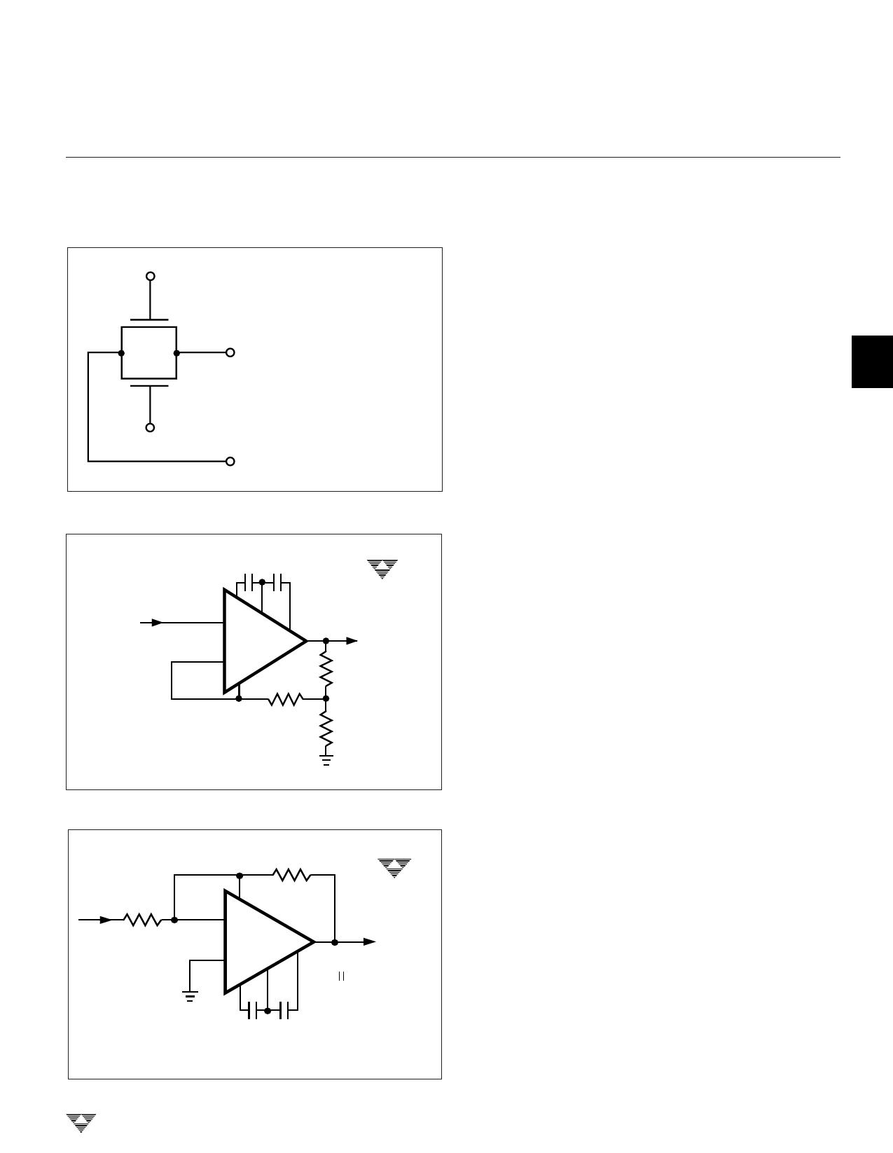
Figure 3. Internal Clamp Circuit
*CONNECT TO VSS
ON 8-PIN DIP.
0.1µF
INPUT
C*
+R
C
–
CLAMP
R3
R3 + ( R1/ R2 ) ≥ 100k Ω
FOR FULL CLAMP EFFECT.
TC7650
OUTPUT
R2
R1
Figure 4. Noninverting Amplifier With Optional Clamp
R1
INPUT
*CONNECT TO VR–
ON 8-PIN DIP.
R2
CLAMP
TC7650
–
C
+ R*
OUTPUT
C
( R1 R2 ) ≥ 100kΩ
FOR FULL CLAMP
EFFECT.
0.1 µF 0.1 µF
Figure 5. Inverting Amplifier with Optional Clamp
TELCOM SEMICONDUCTOR, INC.
The output clamp circuit is shown in Figure 3, with typical
2 inverting and noninverting circuit connections shown in
Figures 4 and 5. Output voltage versus clamp circuit current
characteristics are shown in the typical operating curves.
For the clamp to be fully effective, the impedance across the
clamp output should be greater than 100kΩ.
Latch-Up Avoidance
Junction-isolated CMOS circuits inherently include a
3 parasitic 4-layer (p-n-p-n) structure which has characteris-
tics similar to an SCR. Under certain circumstances this
junction may be triggered into a low-impedance state, result-
ing in excessive supply current. To avoid this condition, no
voltage greater than 0.3V beyond the supply rails should be
applied to any pin. In general, the amplifier supplies must be
established either at the same time or before any input
signals are applied. If this is not possible, the drive circuits
4 must limit input current flow to under 0.1mA to avoid latch-
up.
Thermoelectric Potentials
Precision DC measurements are ultimately limited by
thermoelectric potentials developed in thermocouple junc-
tions of dissimilar metals, alloys, silicon, etc. Unless all
5 junctions are at the same temperature, thermoelectric volt-
ages, typically around 0.1µV/°C, but up to tens of µV/°C for
some materials, will be generated. In order to realize the
benefits extremely-low offset voltages provide, it is essential
to take special precautions to avoid temperature gradients.
All components should be enclosed to eliminate air move-
ment, especially those caused by power-dissipating ele-
ments in the system. Low thermoelectric-coefficient con-
6 nections should be used where possible and power supply
voltages and power dissipation should be kept to a mini-
mum. High-impedance loads are preferable, and separation
from surrounding heat-dissipating elements is advised.
Pin Compatibility
On the 8-pin mini-DIP TC7650, the external null storage
capacitors are connected to pins 1 and 8. On most other
7 operational amplifiers these are left open or are used for
offset potentiometer or compensation capacitor connec-
tions.
For OP05 and OP07 operational amplifiers, the replace-
ment of the offset null potentiometer between pins 1 and 8
by two capacitors from the pins to VSS will convert the OP05/
07 pin configurations for TC7650 operation. For LM108
devices, the compensation capacitor is replaced by the
8 external nulling capacitors. The LM101/748/709 pinouts
are modified similarly by removing any circuit connections to
pin 5. On the TC7650, pin 5 is the output clamp connection.
3-277
Share Link: 