TC7650 查看數據表(PDF) - TelCom Semiconductor, Inc
零件编号
产品描述 (功能)
生产厂家
TC7650 Datasheet PDF : 7 Pages
| |||
TC7650
Other operational amplifiers may use this pin as an offset
or compensation point.
The minor modifications needed to retrofit a TC7650
into existing sockets operating at reduced power supply
voltages make prototyping and circuit verification straight-
forward.
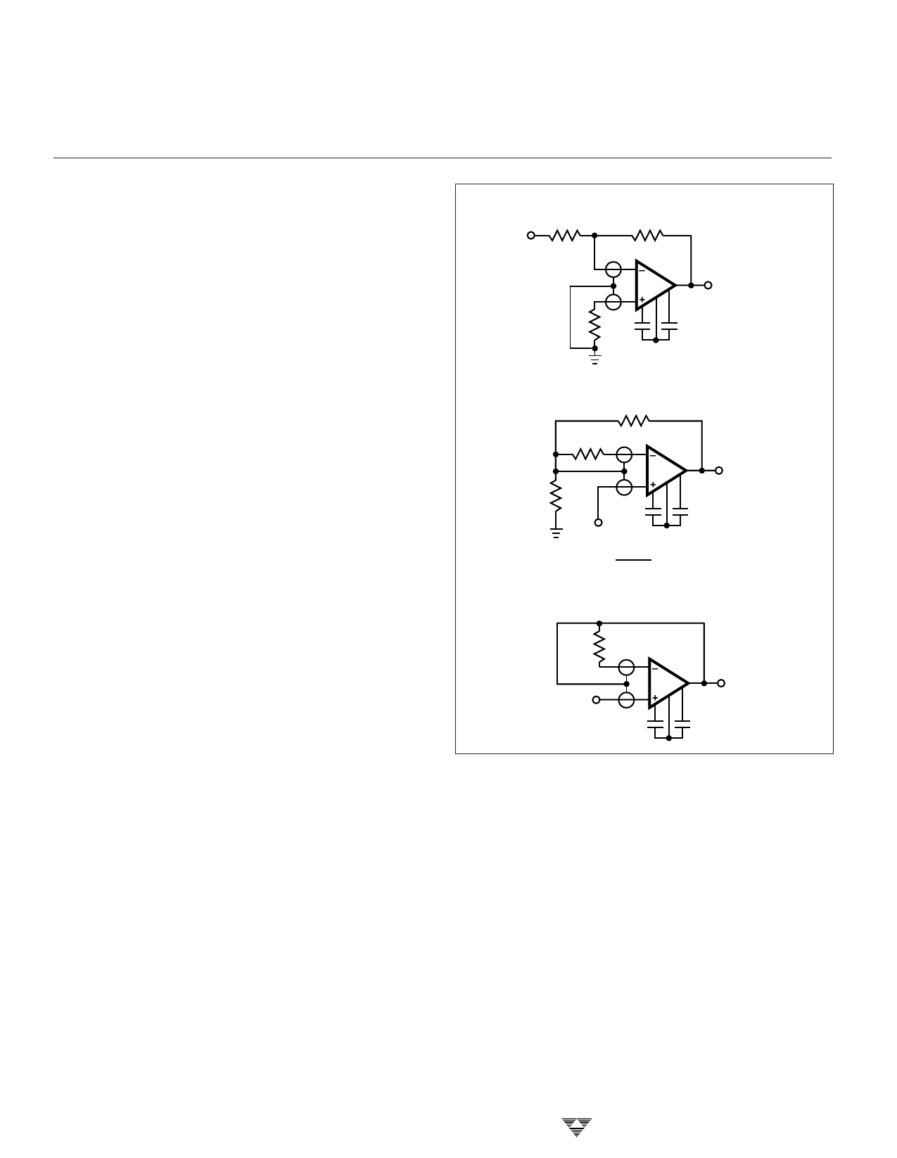
Input Guarding
High impedance, low leakage CMOS inputs allow the
TC7650 to make measurements of high-impedance sources.
Stray leakage paths can increase input currents and de-
crease input resistance unless inputs are guarded. A guard
is a conductive PC trace surrounding the input terminals.
The ring connects to a low-impedance point at the same
potential as the inputs. Stray leakages are absorbed by the
low-impedance ring. The equal potential between ring and
inputs prevents input leakage currents. Typical guard con-
nections are shown in Figure 6.
The 14-pin DIP configuration has been specifically
designed to ease input guarding. The pins adjacent to the
inputs are unused.
In applications requiring low leakage currents, boards
should be cleaned thoroughly and blown dry after soldering.
Protective coatings will prevent future board contamination.
Component Selection
The two required capacitors, CA and CB, have optimum
values, depending on the clock or chopping frequency. For
the preset internal clock, the correct value is 0.1µF. To
maintain the same relationship between the chopping fre-
quency and the nulling time constant, the capacitor values
should be scaled in proportion to the external clock, if used.
High-quality film-type capacitors (such as Mylar) are pre-
ferred; ceramic or other lower-grade capacitors may be
suitable in some applications. For fast settling on initial turn-
on, low dielectric absorption capacitors (such as polypro-
pylene) should be used. With ceramic capacitors, several
seconds may be required to settle to 1µV.
CHOPPER-STABILIZED
OPERATIONAL AMPLIFIER
INPUT
Inverting Amplifier
R1
R2
–
+
R3*
OUTPUT
Noninverting Amplifier
R2
R3*
–
+
R1
OUTPUT
INPUT
NOTE:
R3
=
R1 R2
R1+ R2
SHOULD BE LOW
IMPEDANCE FOR
OPTIMUM GUARDING.
Follower
R3*
–
+
INPUT
OUTPUT
Figure 6. Input Guard Connection
3-278
TELCOM SEMICONDUCTOR, INC.
Share Link: 