LR2905 查看數據表(PDF) - International Rectifier
零件编号
产品描述 (功能)
生产厂家
LR2905 Datasheet PDF : 10 Pages
| |||
IRLR/U2905
Electrical Characteristics @ TJ = 25°C (unless otherwise specified)
Parameter
V(BR)DSS Drain-to-Source Breakdown Voltage
∆V(BR)DSS/∆TJ Breakdown Voltage Temp. Coefficient
RDS(on)
Static Drain-to-Source On-Resistance
VGS(th)
gfs
IDSS
IGSS
Qg
Qgs
Qgd
td(on)
tr
td(off)
tf
LD
LS
Ciss
Coss
Crss
Gate Threshold Voltage
Forward Transconductance
Drain-to-Source Leakage Current
Gate-to-Source Forward Leakage
Gate-to-Source Reverse Leakage
Total Gate Charge
Gate-to-Source Charge
Gate-to-Drain ("Miller") Charge
Turn-On Delay Time
Rise Time
Turn-Off Delay Time
Fall Time
Internal Drain Inductance
Internal Source Inductance
Input Capacitance
Output Capacitance
Reverse Transfer Capacitance
Min. Typ. Max. Units
Conditions
55 ––– ––– V VGS = 0V, ID = 250µA
––– 0.070 ––– V/°C Reference to 25°C, ID = 1mA
––– ––– 0.027
VGS = 10V, ID = 25A
––– ––– 0.030 W VGS = 5.0V, ID = 25A
––– ––– 0.040
VGS = 4.0V, ID = 21A
1.0 ––– 2.0
21 ––– –––
V VDS = VGS, ID = 250µA
S VDS = 25V, ID = 25A
––– ––– 25
––– ––– 250
µA VDS = 55V, VGS = 0V
VDS = 44V, VGS = 0V, TJ = 150°C
––– ––– 100 nA VGS = 16V
––– ––– -100
VGS = -16V
––– ––– 48
ID = 25A
––– ––– 8.6 nC VDS = 44V
––– ––– 25
VGS = 5.0V, See Fig. 6 and 13
––– 11 –––
VDD = 28V
––– 84 ––– ns ID = 25A
––– 26 –––
RG = 3.4Ω, VGS = 5.0V
––– 15 –––
RD = 1.1Ω, See Fig. 10
Between lead,
D
––– 4.5 ––– nH 6mm (0.25in.)
––– 7.5 –––
from package
G
and center of die contact
S
––– 1700 –––
VGS = 0V
––– 400 ––– pF VDS = 25V
––– 150 –––
ƒ = 1.0MHz, See Fig. 5
Source-Drain Ratings and Characteristics
Parameter
IS
Continuous Source Current
(Body Diode)
ISM
Pulsed Source Current
(Body Diode)
VSD
Diode Forward Voltage
trr
Reverse Recovery Time
Qrr
Reverse RecoveryCharge
ton
Forward Turn-On Time
Notes:
Repetitive rating; pulse width limited by
max. junction temperature. ( See fig. 11 )
VDD = 25V, starting TJ = 25°C, L =470µH
RG = 25Ω, IAS = 25A. (See Figure 12)
ISD ≤ 25A, di/dt ≤ 270A/µs, VDD ≤ V(BR)DSS,
TJ ≤ 175°C
Pulse width ≤ 300µs; duty cycle ≤ 2%.
2
Min. Typ. Max. Units
Conditions
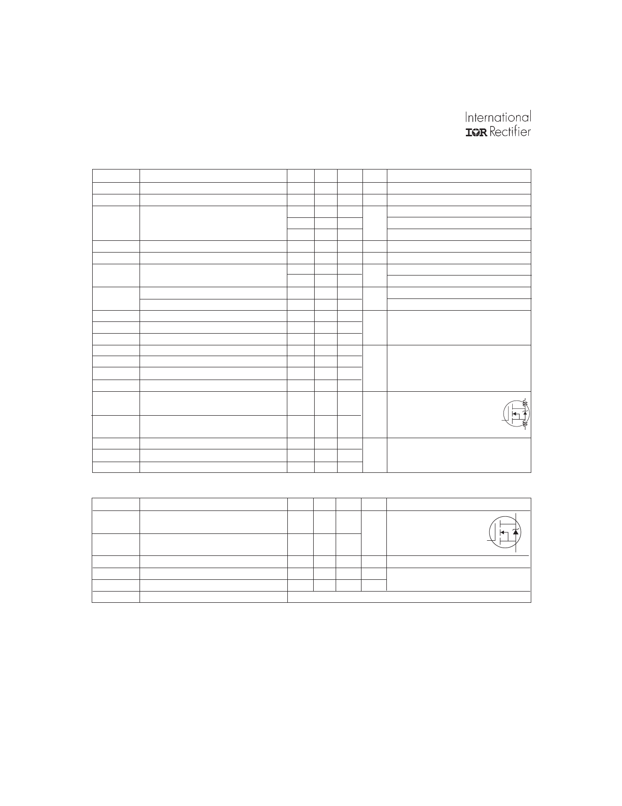
MOSFET symbol
D
––– ––– 42
A
showing the
integral reverse
G
––– ––– 160
p-n junction diode.
S
––– ––– 1.3 V TJ = 25°C, IS = 25A, VGS = 0V
––– 80 120 ns TJ = 25°C, IF = 25A
––– 210 320 nC di/dt = 100A/µs
Intrinsic turn-on time is negligible (turn-on is dominated by LS+LD)
Caculated continuous current based on maximum allowable
junction temperature; Package limitation current = 20A.
This is applied for I-PAK, LS of D-PAK is measured between
lead and center of die contact.
Uses IRLZ44N data and test conditions.
www.irf.com
Share Link: 