MAX19700 查看數據表(PDF) - Maxim Integrated
零件编号
产品描述 (功能)
生产厂家
MAX19700 Datasheet PDF : 32 Pages
| |||
7.5Msps, Ultra-Low-Power
Analog Front-End
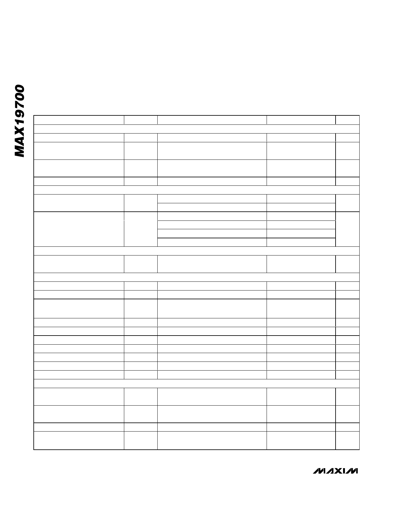
ELECTRICAL CHARACTERISTICS (continued)
(VDD = 3V, OVDD = 1.8V, internal reference (1.024V), CL ≈ 10pF on all digital outputs, fCLK = 7.5MHz (50% duty cycle), ADC input
amplitude = -0.5dBFS, DAC output amplitude = 0dBFS, differential ADC input, differential DAC output, CREFP = CREFN = CCOM =
0.33µF. Typical values are at TA = +25°C, unless otherwise noted. CL < 5pF on all aux-DAC outputs.) (Note 1)
PARAMETER
SYMBOL
CONDITIONS
TRANSMIT-PATH INTERCHANNEL CHARACTERISTICS
I-to-Q Output Isolation
fOUTx,Y = 500kHz, fOUTx,Y = 620kHz
Gain Mismatch Between DAC
Outputs
Measured at DC
MIN TYP MAX UNITS
85
dB
-0.3 ±0.05 +0.3
dB
Phase Mismatch Between DAC
Outputs
fOUT = 620kHz, fCLK = 7.5MHz
Differential Output Impedance
TRANSMIT-PATH ANALOG OUTPUT
Full-Scale Output Voltage
(Table 6)
Bit E7 = 0 (default)
VFS
Bit E7 = 1
Bits CM1 = 0, CM0 = 0 (default)
Output Common-Mode Voltage
(Table 8)
Bits CM1 = 0, CM0 = 1
Bits CM1 = 1, CM0 = 0
Bits CM1 = 1, CM0 = 1
RECEIVE TRANSMIT-PATH INTERCHANNEL CHARACTERISTICS
Receive Transmit Isolation
ADC fINI = fINQ = 1.875MHz, DAC fOUTI =
fOUTQ = 620kHz, fCLK = 7.5MHz
AUXILIARY DACs (DAC1, DAC2, DAC3)
Resolution
(Note 6)
Integral Nonlinearity
INL
±0.16
800
±410
±500
1.32 1.4
1.25
1.1
0.9
85
12
±1.25
D eg r ees
Ω
mV
1.48
V
dB
Bits
LSB
Differential Nonlinearity
DNL
Guaranteed monotonic over codes 100 to
4000 (Note 6)
±0.65
LSB
Gain Error
GE
Zero-Code Error
Output-Voltage Low
VOL
Output-Voltage High
VOH
DC Output Impedance
Settling Time
Glitch Impulse
Rx ADC-Tx DAC TIMING CHARACTERISTICS
CLK Rise to Channel-I Output Data
Valid
tDOI
RL > 200kΩ
RL > 200kΩ
RL > 200kΩ
DC output at midscale
From 1/4 FS to 3/4 FS
From 0 to FS transition
Figure 3 (Note 6)
±0.7
%FS
±0.6
%FS
0.1
V
2.56
V
4
Ω
1
µs
24
nV•s
6.9
10
ns
CLK Fall to Channel-Q Output
Data Valid
CLK Rise/Fall to DR Rise/Fall Time
I-DAC DATA to CLK Fall Setup
Time
tDOQ
tDR
tDSI
Figure 3 (Note 6)
Figure 3 (Note 6)
Figure 5 (Note 6)
9.3
13
ns
8.5
12
ns
10
ns
6 _______________________________________________________________________________________
Share Link: 