AD8230 查看數據表(PDF) - Analog Devices
零件编号
产品描述 (功能)
生产厂家
AD8230 Datasheet PDF : 16 Pages
| |||
AD8230
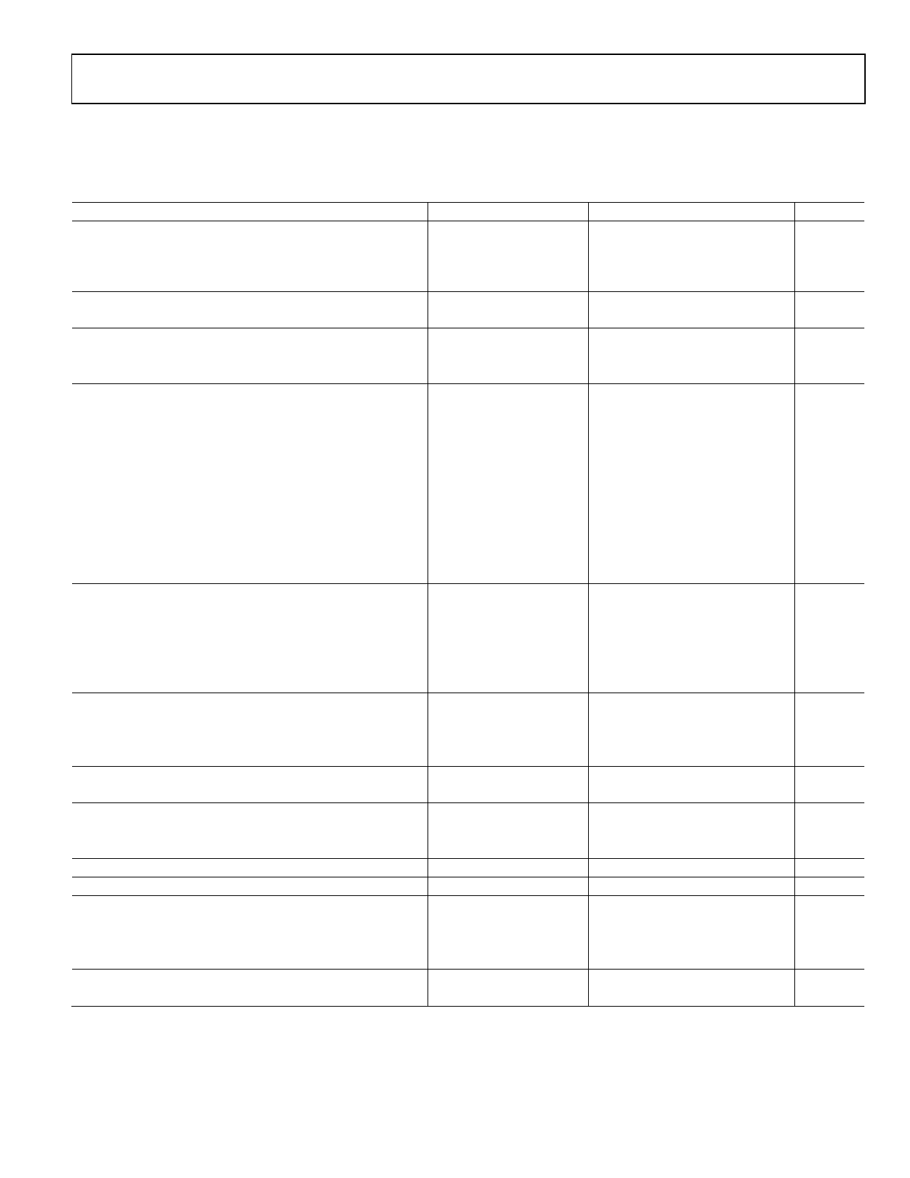
SPECIFICATIONS
VS = ±5 V, VREF = 0 V, RF = 100 kΩ, RG = 1 kΩ (@ TA = 25°C, G = 202, RL = 10 kΩ, unless otherwise noted).
Table 1.
Parameter
VOLTAGE OFFSET
RTI Offset, VOSI
Offset Drift
COMMON-MODE REJECTION (CMR)
CMR to 60 Hz with 1 kΩ Source Imbalance
VOLTAGE OFFSET RTI vs. SUPPLY (PSR)
G=2
G = 202
GAIN
Gain Range
Gain Error2
G=2
G = 10
G = 100
G = 1000
Gain Nonlinearity
Gain Drift
G = 2, 10, 102
G = 1002
INPUT
Input Common-Mode Operating Voltage Range
Over Temperature
Input Differential Operating Voltage Range
Average Input Offset Current3
Average Input Bias Current3
OUTPUT
Output Swing
Over Temperature
Short-Circuit Current
REFERENCE INPUT
Voltage Range4
NOISE
Voltage Noise Density, 1 kHz, RTI
Voltage Noise
SLEW RATE
INTERNAL SAMPLE RATE
POWER SUPPLY
Operating Range (Dual Supplies)
Operating Range (Single Supply)
Quiescent Current
TEMPERATURE RANGE
Specified Performance
Conditions
V+IN = V−IN = 0 V
V+IN = V−IN = 0 V,
TA = −40°C to +125°C
VCM = −5 V to +5 V
G = 2(1 + RF/RG)
T = −40°C to +125°C
VCM = 0 V
VCM = 0 V
T = −40°C to +125°C
VIN+, VIN−, VREF = 0 V
f = 0.1 Hz to 10 Hz
VIN = 500 mV, G = 10
T = −40°C to +125°C
Min
Typ Max
Unit
10
μV
50
nV/°C
110
120
120
101
−VS
−VS
−VS + 0.1
−VS + 0.1
−VS + 3.5
±4
8
−40
120
120
140
1000
0.01 0.04
0.01 0.04
0.01 0.04
0.02 0.05
20
14
60
+VS
+VS
750
33 300
0.15 1
+VS − 0.2
+VS − 0.2
15
+VS − 2.5
240
3
2
6
±8
16
2.7 3.5
+125
dB
dB
dB
V/V
%
%
%
%
ppm
ppm/°C
ppm/°C
V
V
mV
pA
nA
V
V
mA
V
nV/√Hz
μV p-p
V/μs
kHz
V
V
mA
°C
1 The AD8230 can operate as low as G = 2. However, since the differential input range is limited to approximately 750 mV, the AD8230 configured at G < 10 does not
make use of the full output voltage range.
2 Gain drift is determined by the TC match of the external gain setting resistors.
3 Differential source resistance less than 10 kΩ does not result in voltage offset due to input bias current or mismatched series resistors.
4 For G < 10, the reference voltage range is limited to −VS + 4.24 V to +VS – 2.75 V.
Rev. B | Page 3 of 16
Share Link: 