AD8176ABPZ(2007) жҹҘзңӢж•ёж“ҡиЎЁпјҲPDFпјү - Analog Devices
йӣ¶д»¶зј–еҸ·
дә§е“ҒжҸҸиҝ° (еҠҹиғҪ)
з”ҹдә§еҺӮ家
AD8176ABPZ Datasheet PDF : 32 Pages
| |||
Preliminary Technical Data
ABSOLUTE MAXIMUM RATINGS
Table 12.
Parameter
Analog Supply Voltage (VPOS вҖ“ VNEG)
Digital Supply Voltage (VDD вҖ“ DGND)
Ground Potential Difference
(VNEG вҖ“ DGND)
Maximum Potential Difference
(VDD вҖ“ VNEG)
Common-Mode Analog Input Voltage
Differential Analog Input Voltage
Digital Input Voltage
Output Voltage
(Disabled Analog Output)
Output Short-Circuit Duration
Storage Temperature
Operating Temperature Range
Lead Temperature Range
(Soldering 10 sec)
Junction Temperature
Rating
+6 V
+6 V
+0.5 V to вҖ“2.5 V
+8 V
(VNEG вҖ“ 0.5 V)
to (VPOS + 0.5 V)
Вұ2 V
VDD
(VPOS вҖ“ 1 V) to (VNEG + 1 V)
Momentary
вҲ’65В°C to +125В°C
вҲ’40В°C to +85В°C
300В°C
150В°C
Stresses above those listed under Absolute Maximum Ratings
may cause permanent damage to the device. This is a stress
rating only; functional operation of the device at these or any
other conditions above those indicated in the operational
section of this specification is not implied. Exposure to absolute
maximum rating conditions for extended periods may affect
device reliability.
THERMAL RESISTANCE
ОёJA is specified for the worst-case conditions, that is, a device
soldered in a circuit board for surface-mount packages.
Table 13. Thermal Resistance
Package Type
ОёJA
PBGA
15
Unit
В°C/W
AD8176
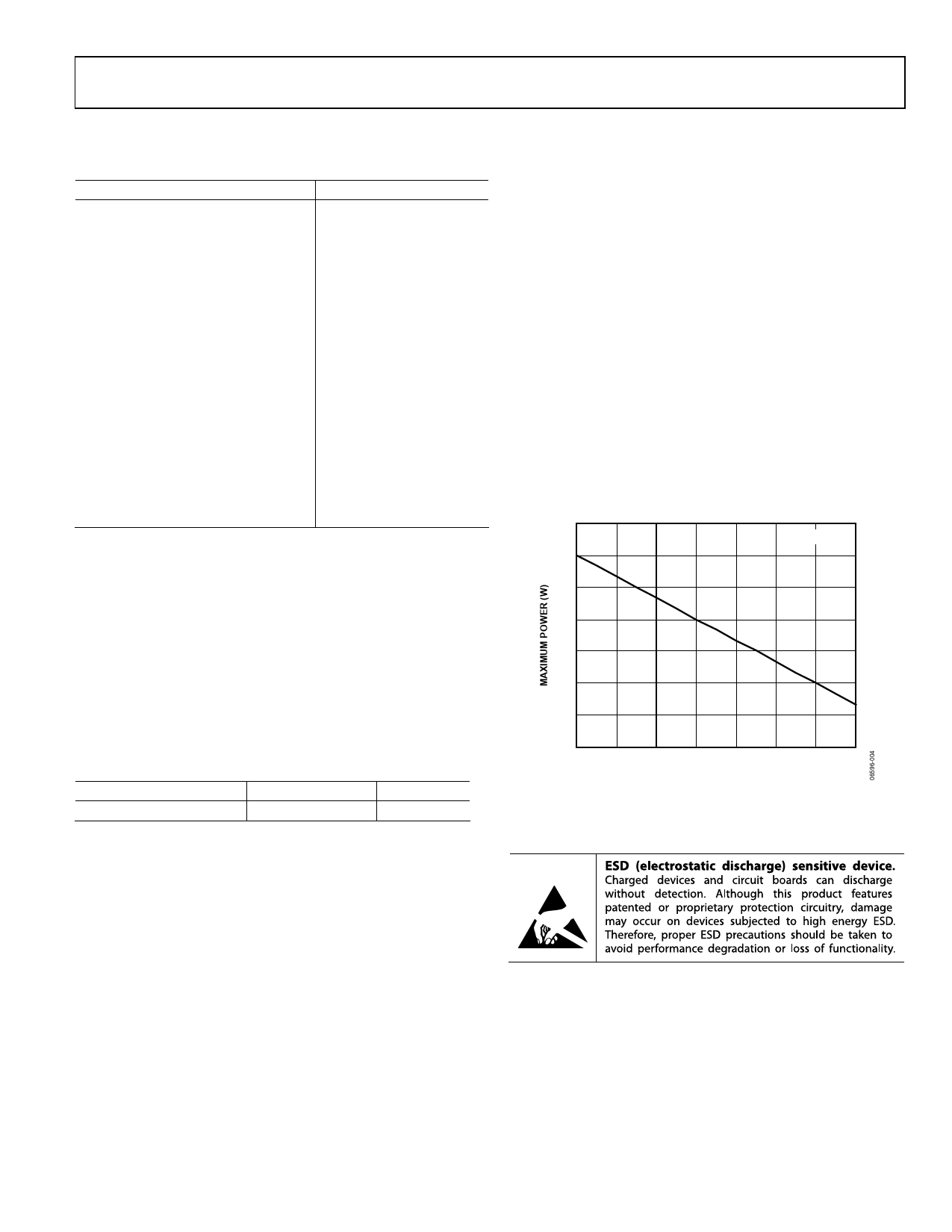
POWER DISSIPATION
The AD8176 is operated with Вұ2.5 V or +5 V supplies and can
drive loads down to 100 О©, resulting in a large range of possible
power dissipations. For this reason, extra care must be taken
derating the operating conditions based on ambient
temperature.
Packaged in a 676-lead BGA, the AD8176 junction-to-ambient
thermal impedance (ОёJA) is 15В°C/W. For long-term reliability,
the maximum allowed junction temperature of the die should
not exceed 150В°C. Temporarily exceeding this limit may cause a
shift in parametric performance due to a change in stresses
exerted on the die by the package. Exceeding a junction
temperature of 175В°C for an extended period can result in
device failure. The following curve shows the range of allowed
internal die power dissipations that meet these conditions over
the вҲ’40В°C to +85В°C ambient temperature range. When using
the table, do not include external load power in the Maximum
Power calculation, but do include load current dropped on the
die output transistors.
8
TJ = 150В°C
7
6
5
4
3
15
25
35
45
55
65
75
85
AMBIENT TEMPERATURE (В°C)
Figure 4. Maximum Die Power Dissipation vs. Ambient Temperature
ESD CAUTION
Rev. PrA | Page 7 of 32
Share Link: 