AD816 查看數據表(PDF) - Analog Devices
零件编号
产品描述 (功能)
生产厂家
AD816 Datasheet PDF : 16 Pages
| |||
AD816
THEORY OF OPERATION (DRIVER)
The AD816 driver is a dual current feedback amplifier with high
(500 mA) output current capability. Being a current feedback
amplifier, the AD816 driver’s open-loop behavior is expressed
as transimpedance, ∆VO/∆I–IN, or TZ. The open-loop trans-
impedance behaves just as the open-loop voltage gain of a volt-
age feedback amplifier, that is, it has a large dc value and de-
creases at roughly 6 dB/octave in frequency.
Since RIN is proportional to 1/gM, the equivalent voltage gain is
just TZ × gM, where the gM in question is the transconductance
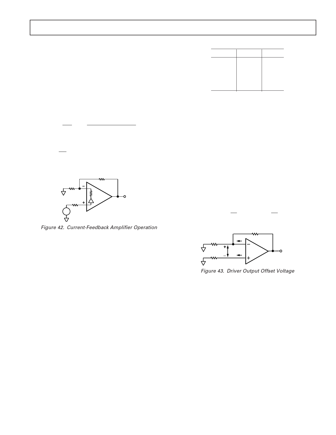
of the input stage. Figure 42 shows the driver connected as a
follower with gain. Basic analysis yields the following results:
( ) VO = G ×
TZ S
( ) VIN
T Z S + G × RIN + RF
where:
G=
1 + RF
RG
RIN = 1/gM ≈ 25 Ω
RG
RN
RF
RIN
VOUT
VIN
Figure 42. Current-Feedback Amplifier Operation
Recognizing that G × RIN << RF for low gains, it can be seen to
the first order that bandwidth for this amplifier is independent
of gain (G).
Considering that additional poles contribute excess phase at
high frequencies, there is a minimum feedback resistance below
which peaking or oscillation may result. This fact is used to
determine the optimum feedback resistance, RF. In practice
parasitic capacitance at the inverting input terminal will also add
phase in the feedback loop so that picking an optimum value for
RF can be difficult.
Achieving and maintaining gain flatness of better than 0.1 dB at
frequencies above 10 MHz requires careful consideration of
several issues.
Choice of Feedback and Gain Resistors
The fine scale gain flatness will, to some extent, vary with
feedback resistance. It is therefore recommended that once
optimum resistor values have been determined, 1% tolerance
values should be used if it is desired to maintain flatness over a
wide range of production lots. Table I shows optimum values
for several useful gain configurations. These should be used as a
starting point in any application.
Table I. Driver Resistor Values
G = +1
–1
+2
+5
+10
RF (⍀)
604
499
499
499
1k
RG (⍀)
∞
499
499
125
110
DRIVER DC ERRORS AND NOISE
There are three major noise and offset terms to consider in a
current feedback amplifier. For offset errors refer to the equa-
tion below. For noise error the terms are root-sum-squared to
give a net output error. In the circuit below (Figure 43), they
are input offset (VIO) which appears at the output multiplied by
the noise gain of the circuit (1 + RF/RG), noninverting input
current (IBN × RN) also multiplied by the noise gain, and the
inverting input current, which when divided between RF and RG
and subsequently multiplied by the noise gain always appear at
the output as IBI × RF. The input voltage noise of the AD816 is
less than 4 nV/√Hz. At low gains, however, the inverting input
current noise times RF is the dominant noise source. Careful
layout and device matching contribute to better offset and drift.
The typical performance curves in conjunction with the equations
below can be used to predict the performance of the AD816 in
any application.
VOUT
= VIO 1 +
RF
RG
±
I BN
RN
1
+
RF
RG
±
I BI
RF
RG
RN VIO
RF
IBI
AD816
IBN DRIVERS
VOUT
Figure 43. Driver Output Offset Voltage
THEORY OF OPERATION (RECEIVER)
Each AD816 receiver is a wide band high performance opera-
tional amplifier. It also provides a constant slew rate, bandwidth
and settling time over its entire specified temperature range.
The AD816 receiver consists of a degenerated NPN differential
pair driving matched PNPs in a folded-cascode gain stage. The
output buffer stage employs emitter followers in a class AB
amplifier which deliver the necessary current to the load while
maintaining low levels of distortion.
A protection resistor in series with the noninverting input is
required in circuits where the input to the receiver could be
subject to transients on continuous overload voltages exceeding
the ± 6 V maximum differential limit. The resistor provides
protection for the input transistors, by limiting their maximum
base current.
REV. B
–11–
Share Link: 