AD816 查看數據表(PDF) - Analog Devices
零件编号
产品描述 (功能)
生产厂家
AD816 Datasheet PDF : 16 Pages
| |||
AD816
ABSOLUTE MAXIMUM RATINGS1
Supply Voltage . . . . . . . . . . . . . . . . . . . . . . . . . . . ± 18 V Total
Internal Power Dissipation2
Plastic (Y, YS and VR) . . 3.05 W (Observe Derating Curves)
Input Voltage (Common Mode) . . . . . . . . . . . . . . . . . . . . ± VS
Differential Input Voltage . . . . . . . . . . . . . . . . . . . . . . . . ± 6 V
Output Short Circuit Duration
. . . . . . . . . . . . . . . . . . . . . . Observe Power Derating Curves
Storage Temperature Range
Y, YS, VR Package . . . . . . . . . . . . . . . . . . –65°C to +125°C
Operating Temperature Range
AD816A . . . . . . . . . . . . . . . . . . . . . . . . . . . –40°C to +85°C
Lead Temperature Range (Soldering, 10 sec) . . . . . . . +300°C
NOTES
1Stresses above those listed under Absolute Maximum Ratings may cause perma-
nent damage to the device. This is a stress rating only. functional operation of the
device at these or any other conditions above those indicated in the operational
section of this specification is not implied. Exposure to absolute maximum rating
conditions for extended periods may affect device reliability.
2Specification is for device in free air: 15-Lead Through Hole and Surface Mount:
θJA = 41°C/W.
PIN CONFIGURATION
Y-15
VR-15, YS-15
TOP VIEW
TOP VIEW
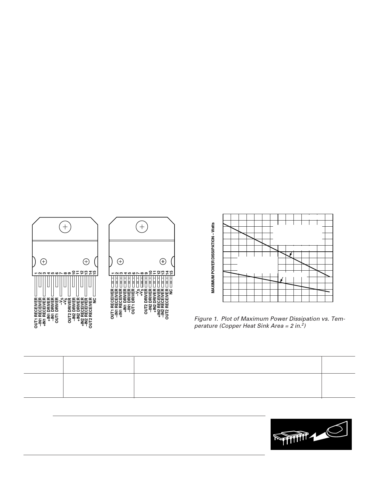
MAXIMUM POWER DISSIPATION
The maximum power that can be safely dissipated by the
AD816 is limited by the associated rise in junction temperature.
The maximum safe junction temperature for the plastic encap-
sulated parts is determined by the glass transition temperature
of the plastic, about 150°C. Exceeding this limit temporarily
may cause a shift in parametric performance due to a change in
the stresses exerted on the die by the package. Exceeding a
junction temperature of 175°C for an extended period can result
in device failure.
The AD816 has thermal shutdown protection, which guarantees
that the maximum junction temperature of the die remains below a
safe level. However, shorting the output to ground or either power
supply for an indeterminate period will result in device failure.
To ensure proper operation, it is important to observe the derat-
ing curves and refer to the section on power considerations.
It must also be noted that in high (noninverting) gain configura-
tions (with low values of gain resistor), a high level of input
overdrive can result in a large input error current, which may
result in a significant power dissipation in the input stage. This
power must be included when computing the junction tempera-
ture rise due to total internal power.
14
TJ = 150؇C
13
12
θJA = 16؇C/W
11
SOLDERED DOWN TO
10
COPPER HEAT SINK AREA
(STILL AIR = 0FT/MIN)
9
AD816 AVR, AY
8
7
θJA = 41؇C/W
6
(STILL AIR = 0FT/MIN)
5
NO HEAT SINK
4
AD816 AVR, AY
3
2
1
0
–50 –40 –30 –20 –10 0 10 20 30 40 50 60 70 80 90
AMBIENT TEMPERATURE – ؇C
Figure 1. Plot of Maximum Power Dissipation vs. Tem-
perature (Copper Heat Sink Area = 2 in.2)
Model
AD816AY
AD816AYS
AD816AVR
Temperature Range
–40°C to +85°C
–40°C to +85°C
–40°C to +85°C
ORDERING GUIDE
Package Description
15-Lead Through-Hole SIP with Staggered Leads and 90° Lead Form
15-Lead Through-Hole SIP with Staggered Leads and Straight Lead Form
15-Lead Surface Mount DDPAK
Package
Option
Y-15
YS-15
VR-15
CAUTION
ESD (electrostatic discharge) sensitive device. Electrostatic charges as high as 4000 V readily
accumulate on the human body and test equipment and can discharge without detection.
Although the AD816 features proprietary ESD protection circuitry, permanent damage may
occur on devices subjected to high energy electrostatic discharges. Therefore, proper ESD
precautions are recommended to avoid performance degradation or loss of functionality.
WARNING!
ESD SENSITIVE DEVICE
–4–
REV. B
Share Link: 