MMBZ6V8ALT1G 查看數據表(PDF) - ON Semiconductor
零件编号
产品描述 (功能)
生产厂家
MMBZ6V8ALT1G Datasheet PDF : 7 Pages
| |||
MMBZxxxALT1G Series, SZMMBZxxxALT1G Series
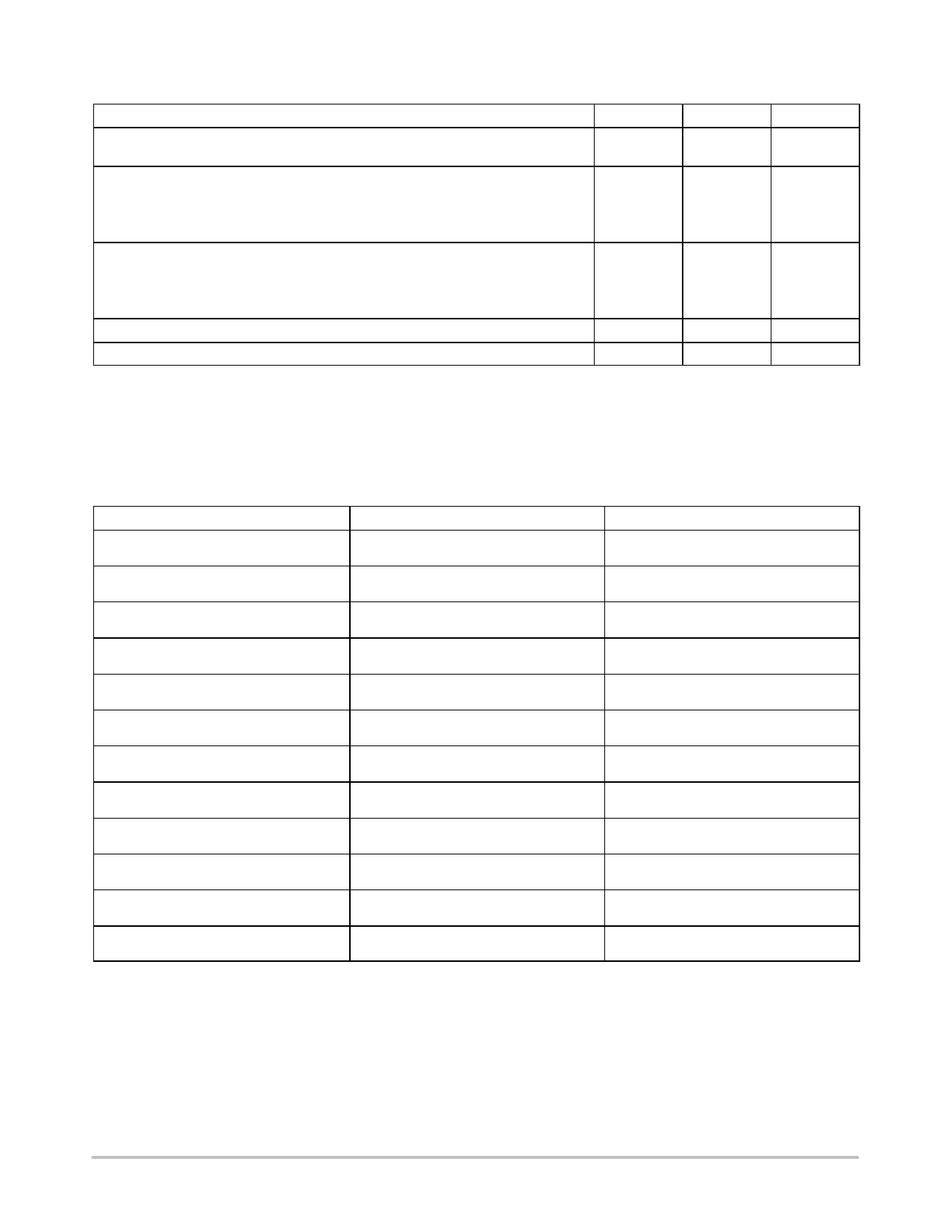
MAXIMUM RATINGS
Rating
Symbol
Value
Unit
Peak Power Dissipation @ 1.0 ms (Note 1) MMBZ5V6ALT1G thru MMBZ9V1ALT1G
@ TL 25C
MMBZ12VALT1G thru MMBZ33VALT1G
Total Power Dissipation on FR−5 Board (Note 2)
@ TA = 25C
Derate above 25C
Ppk
PD
24
W
40
225
mW
1.8
mW/C
Thermal Resistance Junction−to−Ambient
Total Power Dissipation on Alumina Substrate (Note 3)
@ TA = 25C
Derate above 25C
RqJA
PD
556
C/W
300
mW
2.4
mW/C
Thermal Resistance Junction−to−Ambient
RqJA
417
C/W
Junction and Storage Temperature Range
TJ, Tstg
− 55 to +150
C
Lead Solder Temperature − Maximum (10 Second Duration)
TL
260
C
Stresses exceeding Maximum Ratings may damage the device. Maximum Ratings are stress ratings only. Functional operation above the
Recommended Operating Conditions is not implied. Extended exposure to stresses above the Recommended Operating Conditions may affect
device reliability.
1. Non−repetitive current pulse per Figure 6 and derate above TA = 25C per Figure 7.
2. FR−5 = 1.0 x 0.75 x 0.62 in.
3. Alumina = 0.4 x 0.3 x 0.024 in, 99.5% alumina.
*Other voltages may be available upon request.
ORDERING INFORMATION
Device
Package
Shipping†
MMBZ5V6ALT1G
SOT−23
(Pb−Free)
3,000 / Tape & Reel
SZMMBZ5V6ALT1G
SOT−23
(Pb−Free)
3,000 / Tape & Reel
MMBZ5V6ALT3G
SOT−23
(Pb−Free)
10,000 / Tape & Reel
MMBZ6VxALT1G
SOT−23
(Pb−Free)
3,000 / Tape & Reel
SZMMBZ6VxALT1G
SOT−23
(Pb−Free)
3,000 / Tape & Reel
MMBZ6VxALT3G
SOT−23
(Pb−Free)
10,000 / Tape & Reel
MMBZ9V1ALT1G
SOT−23
(Pb−Free)
3,000 / Tape & Reel
MMBZ9V1ALT13G
SOT−23
(Pb−Free)
10,000 / Tape & Reel
MMBZxxVALT1G
SOT−23
(Pb−Free)
3,000 / Tape & Reel
SZMMBZxxVALT1G
SOT−23
(Pb−Free)
3,000 / Tape & Reel
MMBZxxVALT3G
SOT−23
(Pb−Free)
10,000 / Tape & Reel
SZMMBZxxVALT3G
SOT−23
(Pb−Free)
10,000 / Tape & Reel
†For information on tape and reel specifications, including part orientation and tape sizes, please refer to our Tape and Reel Packaging
Specifications Brochure, BRD8011/D.
http://onsemi.com
2
Share Link: 