OKY-T/5-D12N-C 查看數據表(PDF) - Murata Power Solutions
零件编号
产品描述 (功能)
生产厂家
OKY-T/5-D12N-C Datasheet PDF : 21 Pages
| |||
OKY-T/3,T/5-D12 Series
Adjustable Output 3 and 5-Amp DOSA-SMT DC/DC Converters
Specification Notes, Cont.:
(5) The On/Off Control Input should use either a switch or an open collector/open drain transistor referenced
to -Input Common. A logic gate may also be used by applying appropriate external voltages which do not
exceed +Vin.
(6) Short circuit shutdown begins when the output voltage degrades approximately 2% from the selected
setting.
(7) For W5 models, the Input Voltage must exceed the Output Voltage at all times by the ratio of Vin >= (1.15 x
Vout). Please see the separate W5 data sheet.
(8) Output noise may be further reduced by adding an external filter. At zero output current, the output may
contain low frequency components which exceed the ripple specification. The output may be operated
indefinitely with no load.
(9) All models are fully operational and meet published specifications, including “cold start” at –40˚ C.
(10) Regulation specifications describe the deviation as the line input voltage or output load current is varied
from a nominal midpoint value to either extreme.
(11) Other input or output voltage ranges will be reviewed under scheduled quantity special order.
(12) Maximum PC board temperature is measured with the sensor in the center of the converter.
(13) Do not exceed maximum power specifications when adjusting the output trim.
(14) The maximum output capacitive loads depend on the the Equivalent Series Resistance (ESR) of the external
output capacitor and, to a lesser extent, the distance and series impedance to the load. Larger caps will
reduce output noise but may change the transient response. Newer ceramic caps with very low ESR may
require lower capacitor values to avoid instability. Thoroughly test your capacitors in the application. Please
refer to the Output Capacitive Load Application Note.
(15) Do not allow the input voltage to degrade lower than the input undervoltage shutdown voltage at all times.
Otherwise, you risk having the converter turn off. The undervoltage shutdown is not latching and will
attempt to recover when the input is brought back into normal operating range.
(16) The outputs are not intended to sink appreciable reverse current.
(17) “Hiccup” overcurrent operation repeatedly attempts to restart the converter with a brief, full-current output.
If the overcurrent condition still exists, the restart current will be removed and then tried again. This short
current pulse prevents overheating and damaging the converter. Once the fault is removed, the converter
immediately recovers normal operation.
Output Voltage Adustment
The output voltage may be adjusted over a limited range by connecting an
external trim resistor (Rtrim) between the Trim pin and Ground. The Rtrim
resistor must be a 1/10 Watt precision metal film type, ±1% accuracy or
better with low temperature coefficient, ±100 ppm/oC. or better. Mount the
resistor close to the converter with very short leads or use a surface mount
trim resistor.
In the tables below, the calculated resistance is given. Do not exceed the
specified limits of the output voltage or the converter’s maximum power
rating when applying these resistors. Also, avoid high noise at the Trim
input. However, to prevent instability, you should never connect any capaci-
tors to Trim.
OKY-T/3-D12, -T/5-D12
Output Voltage
5.0 V.
3.3 V.
2.5 V.
2.0 V.
1.8 V.
1.5 V.
1.2 V.
1.0 V.
0.7525 V.
Calculated Rtrim (KΩ)
1.472
3.122
5.009
7.416
9.024
13.05
22.46
41.424
∞ (open)
Resistor Trim Equation, D12 models:
RTRIM () = ______1_0_5_0_0___ –1000
VOUT – 0.7525V
www.murata-ps.com/support
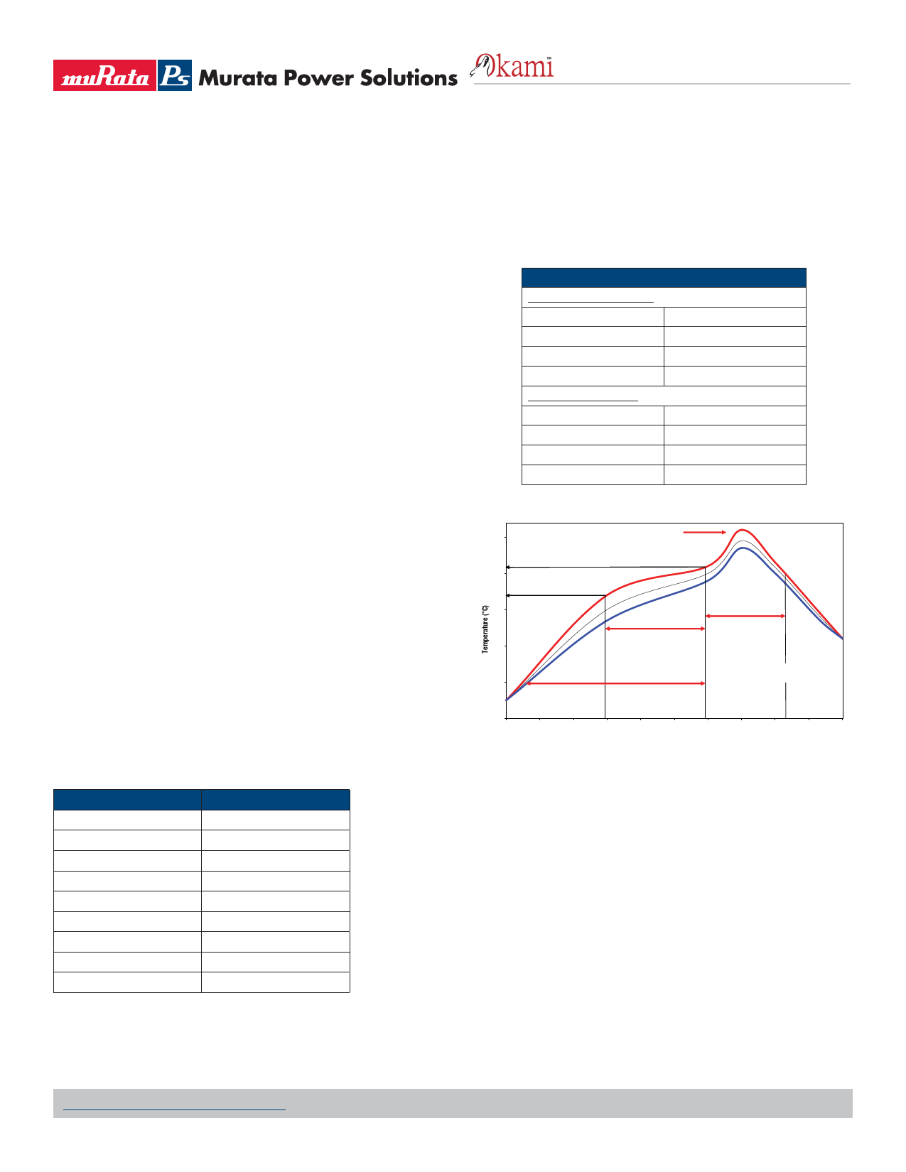
Soldering Guidelines
Murata Power Solutions recommends the specifications below when installing these
converters. These specifications vary depending on the solder type. Exceeding these
specifications may cause damage to the product. Your production environment
may differ therefore please thoroughly review these guidelines with your process
engineers.
Reflow Solder Operations for surface-mount products (SMT)
For Sn/Ag/Cu based solders:
Preheat Temperature
Less than 1 ºC. per second
Time over Liquidus
45 to 75 seconds
Maximum Peak Temperature 260 ºC.
Cooling Rate
Less than 3 ºC. per second
For Sn/Pb based solders:
Preheat Temperature
Less than 1 ºC. per second
Time over Liquidus
60 to 75 seconds
Maximum Peak Temperature 235 ºC.
Cooling Rate
Less than 3 ºC. per second
Recommended Lead-free Solder Reflow Profile
250
Peak Temp.
235-260° C
200
150
Reflow Zone
Soaking Zone
time above 217° C
120 sec max
45-75 sec
100
<1.5° C/sec
Preheating Zone
50
240 sec max
High trace = normal upper limit
Low trace = normal lower limit
0
0
30
60
90
120
150
180
210
240
270
300
Time (sec)
High trace = normal upper limit
Low trace - normal lower limit
MDC_OKY-T/3,T/5-D12 Series.B15 Page 5 of 21
Share Link: 