TQ9147B 查看數據表(PDF) - TriQuint Semiconductor
零件编号
产品描述 (功能)
生产厂家
TQ9147B Datasheet PDF : 10 Pages
| |||
TQ9147B
Data Sheet
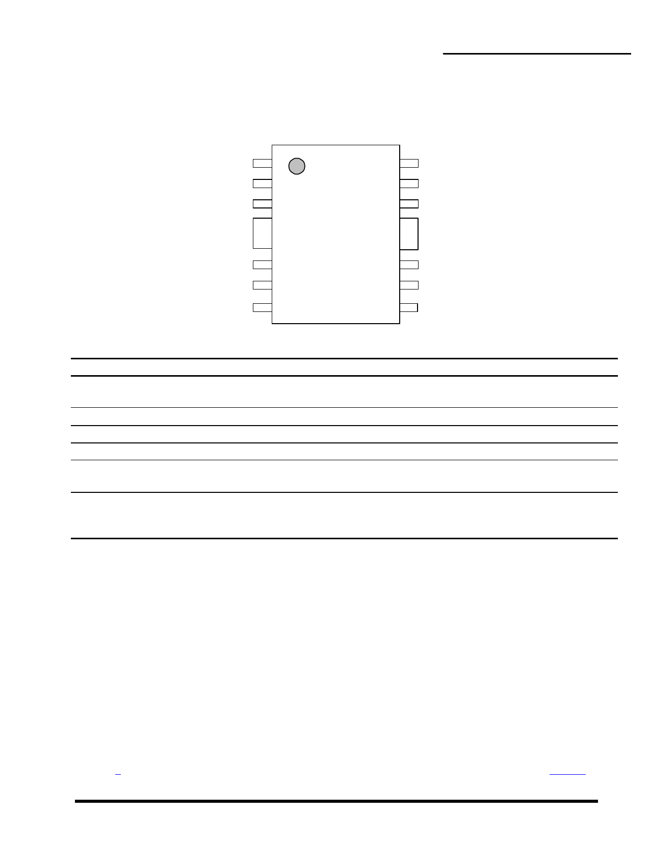
Package Pinout
RFOUT 1
GND 2
VG3 3
GND 4
5
RFIN 6
GND 7
VG1 8
TQ9147B
16 RFOUT
15 GND
14 VD2
13
GND
12
11 VG2
10 GND
9 VD1
Pin Descriptions
Pin Name
RFOUT
RFIN
VG1
VD1
VG2
GND
Pin #
1,16
6
8
9
11
2, 3, 4, 5, 7,
10, 12, 13,
14, 15
Description and Usage
Power Amplifier output and second-stage supply voltage. Critical, but simple, matching circuit required. Bias choke for VD2
required, local bypass cap recommend, and DC blocking capacitor required.
RF input to power amplifier. Matched to 50 Ω. Internal DC block.
First stage gate voltage. Local bypass cap needed. Set VG1 = -1.5 V or use bias stabilization circuit.
First stage supply voltage. Local bypass cap recommended. Use same voltage as VD2 or use bias stabilization circuit.
Second stage gate voltage. Local bypass cap needed. Required 50 Ω series resistor near device for stability. Set
VG2 = -2.2 V or use bias stabilization circuit.
Ground connections. Provide thermal path for heat dissipation and RF grounding. Very important to place multiple via holes
immediately adjacent to the pins.
Revision AA
TQS Wireless Communications • 2300 NE Brookwood Parkway
8900
• Hillsboro, OR 97124
• (503) 615-9000
June 30November, 1998
• FAX:(503) 615-
Share Link: 