DS1340-18 查看數據表(PDF) - Dallas Semiconductor -> Maxim Integrated
零件编号
产品描述 (功能)
生产厂家
DS1340-18 Datasheet PDF : 13 Pages
| |||
I2C RTC with Trickle Charger
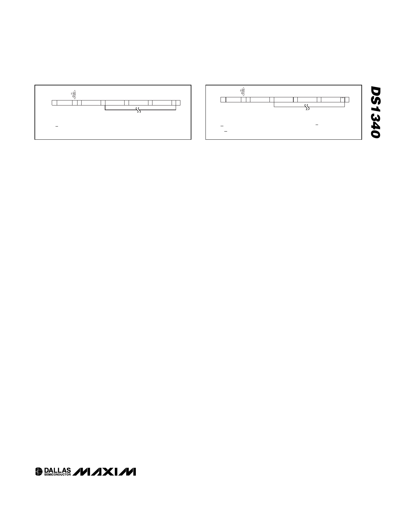
<SLAVE
<WORD
ADDRESS> ADDRESS (n)> <DATA (n)> <DATA (n + 1)> <DATA (n + X)>
S 1101000 0 A XXXXXXXX A XXXXXXXX A XXXXXXXX A XXXXXXXX A P
S — START
A — ACKNOWLEDGE
P — STOP
DATA TRANSFERRED
(X + 1 BYTES + ACKNOWLEDGE)
R/W — READ/WRITE OR DIRECTION BIT ADDRESS = D0H
Figure 8. Slave Receiver Mode (Write Mode)
Accordingly, the following bus conditions have been
defined:
Bus not busy: Both data and clock lines remain
high.
START data transfer: A change in the data line’s
state from high to low, while the clock line is high,
defines a START condition.
STOP data transfer: A change in the data line’s
state from low to high, while the clock line is high,
defines a STOP condition.
Data valid: The data line’s state represents valid
data when, after a START condition, the data line is
stable for the duration of the high period of the
clock signal. The data on the line must be changed
during the low period of the clock signal. There is
one clock pulse per bit of data.
Each data transfer is initiated with a START condi-
tion and terminated with a STOP condition. The
number of data bytes transferred between the
START and STOP conditions is not limited, and is
determined by the master device. The information
is transferred byte-wise and each receiver
acknowledges with a ninth bit.
Acknowledge: Each receiving device, when
addressed, is obliged to generate an acknowl-
edge after the reception of each byte. The master
device must generate an extra clock pulse that is
associated with this acknowledge bit.
A device that acknowledges must pull down the
SDA line during the acknowledge clock pulse in
such a way that the SDA line is stable low during
the high period of the acknowledge-related clock
pulse. Setup and hold times must be taken into
account. A master must signal an end of data to
the slave by not generating an acknowledge bit on
the last byte that has been clocked out of the
slave. In this case, the slave must leave the data
line high to enable the master to generate the
STOP condition.
<SLAVE
ADDRESS>
<DATA (n)> <DATA (n + 1)> <DATA (n + 2)> <DATA (n + X)>
S 1101000 1 A XXXXXXXX A XXXXXXXX A XXXXXXXX A XXXXXXXX A P
S — START
A — ACKNOWLEDGE
P — STOP
A — NOT ACKNOWLEDGE
DATA TRANSFERRED
(X + 1 BYTES + ACKNOWLEDGE)
NOTE: LAST DATA BYTE IS FOLLOWED BY
A NOT ACKNOWLEDGE (A) SIGNAL
R/W — READ/WRITE OR DIRECTION BIT ADDRESS = D0H
Figure 9. Slave Transmitter Mode (Read Mode
Figures 8 and 9 detail how data transfer is accom-
plished on the I2C bus. Depending upon the state of
the R/W bit, two types of data transfer are possible:
Data transfer from a master transmitter to a
slave receiver. The first byte transmitted by the
master is the slave address. Next follows a num-
ber of data bytes. The slave returns an acknowl-
edge bit after each received byte.
Data transfer from a slave transmitter to a mas-
ter receiver. The master transmits the first byte (the
slave address). The slave then returns an acknowl-
edge bit. Next follows a number of data bytes trans-
mitted by the slave to the master. The master
returns an acknowledge bit after all received bytes
other than the last byte. At the end of the last
received byte, a not acknowledge is returned.
The master device generates all the serial clock
pulses and the START and STOP conditions. A
transfer is ended with a STOP condition or with a
repeated START condition. Since a repeated
START condition is also the beginning of the next
serial transfer, the bus is not released.
The DS1340 can operate in the following two modes:
Slave Receiver Mode (Write Mode): Serial data
and clock are received through SDA and SCL.
After each byte is received, an acknowledge bit is
transmitted. Start and STOP conditions are recog-
nized as the beginning and end of a serial trans-
fer. Hardware performs address recognition after
reception of the slave address and direction bit.
The slave address byte is the first byte received
after the master generates the START condition.
The slave address byte contains the 7-bit DS1340
address, which is 1101000, followed by the direc-
tion bit (R/W), which is 0 for a write. After receiving
and decoding the slave address byte, the DS1340
outputs an acknowledge on SDA. After the
DS1340 acknowledges the slave address + write
bit, the master transmits a word address to the
DS1340. This sets the register pointer on the
DS1340, with the DS1340 acknowledging the
transfer. The master can then transmit zero or
____________________________________________________________________ 11
Share Link: 