22RIA 查看數據表(PDF) - Vishay Semiconductors
零件编号
产品描述 (功能)
生产厂家
22RIA Datasheet PDF : 8 Pages
| |||
www.vishay.com
VS-22RIA Series
Vishay Semiconductors
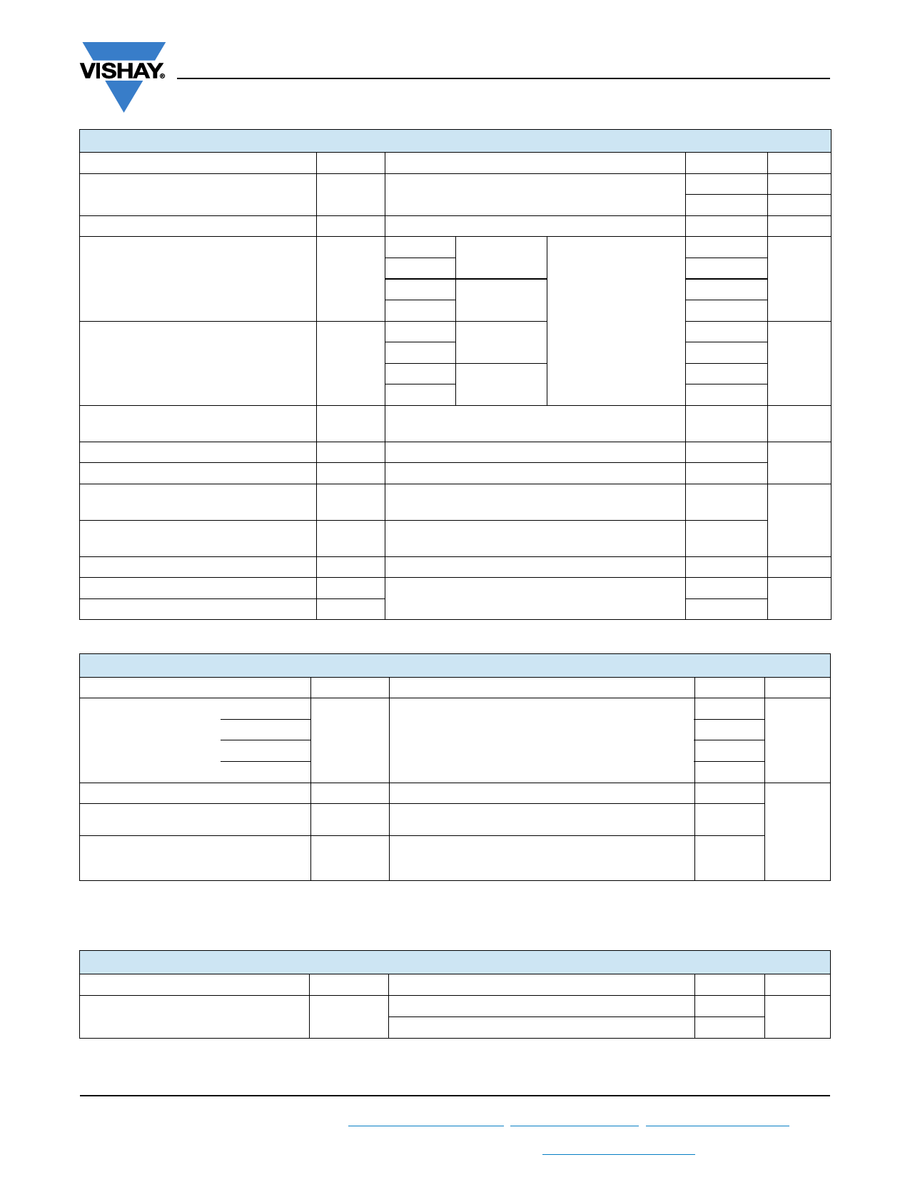
ABSOLUTE MAXIMUM RATINGS
PARAMETER
SYMBOL
Maximum average on-state current
at case temperature
IT(AV)
Maximum RMS on-state current
IT(RMS)
Maximum peak, one-cycle
non-repetitive surge current
ITSM
Maximum I2t for fusing
I2t
Maximum I2t for fusing
Low level value of threshold voltage
High level value of threshold voltage
Low level value of
on-state slope resistance
High level value of
on-state slope resistance
Maximum on-state voltage
Maximum holding current
Latching current
I2t
VT(TO)1
VT(TO)2
rt1
rt2
VTM
IH
IL
TEST CONDITIONS
180° sinusoidal conduction
t = 10 ms No voltage
t = 8.3 ms reapplied
t = 10 ms
t = 8.3 ms
t = 10 ms
t = 8.3 ms
100 % VRRM
reapplied
No voltage
reapplied
Sinusoidal half wave,
initial TJ =TJ maximum
t = 10 ms 100 % VRRM
t = 8.3 ms reapplied
t = 0.1 to 10 ms, no voltage reapplied,
TJ = TJ maximum
(16.7 % x x IT(AV) < I < x IT(AV)), TJ = TJ maximum
(I > x IT(AV)), TJ = TJ maximum
(16.7 % x x IT(AV) < I < x IT(AV)), TJ = TJ maximum
(I > x IT(AV)), TJ = TJ maximum
Ipk = 70 A, TJ = 25 °C
TJ = 25 °C, anode supply 6 V, resistive load
VALUES
22
85
35
400
420
335
355
793
724
560
515
7930
0.83
0.95
14.9
13.4
1.70
130
200
UNITS
A
°C
A
A
A2s
A2s
V
m
V
mA
SWITCHING
PARAMETER
SYMBOL
TEST CONDITIONS
VALUES
Maximum rate of rise
of turned-on current
Typical turn-on time
VDRM 600 V
VDRM 800 V
VDRM 1000 V
VDRM 1600 V
Typical reverse recovery time
Typical turn-off time
dI/dt
tgt
trr
tq
200
TJ = TJ maximum, VDM = Rated VDRM
180
Gate pulse = 20 V, 15 , tp = 6 μs, tr = 0.1 μs maximum
ITM = (2 x rated dI/dt) A
160
150
TJ = 25 °C, at rated VDRM/VRRM, TJ = 125 °C
0.9
TJ = TJ maximum, ITM = IT(AV), tp > 200 μs,
dI/dt = - 10 A/μs
4
TJ = TJ maximum, ITM = IT(AV), tp > 200 μs, VR = 100 V,
dI/dt = - 10 A/μs, dV/dt = 20 V/μs linear to 67 % VDRM, 110
gate bias 0 V to 100 W
Note
• tq = 10 μs up to 600 V, tq = 30 μs up to 1600 V available on special request
UNITS
A/μs
μs
BLOCKING
PARAMETER
SYMBOL
TEST CONDITIONS
Maximum critical rate of rise
of off-state voltage
dV/dt
TJ = TJ maximum linear to 100 % rated VDRM
TJ = TJ maximum linear to 67 % rated VDRM
Note
(1) Available with: dV/dt = 1000 V/μs, to complete code add S90 i.e. 22RIA120S90
VALUES
100
300 (1)
UNITS
V/μs
Revision: 21-Sep-17
2
Document Number: 93700
For technical questions within your region: DiodesAmericas@vishay.com, DiodesAsia@vishay.com, DiodesEurope@vishay.com
THIS DOCUMENT IS SUBJECT TO CHANGE WITHOUT NOTICE. THE PRODUCTS DESCRIBED HEREIN AND THIS DOCUMENT
ARE SUBJECT TO SPECIFIC DISCLAIMERS, SET FORTH AT www.vishay.com/doc?91000
Share Link: 