23C256 وں¥çœ‹و•¸و“ڑè،¨ï¼ˆPDF) - Holtek Semiconductor
零ن»¶ç¼–هڈ·
ن؛§ه“پوڈڈè؟° (هٹں能)
ç”ںن؛§هژ‚ه®¶
23C256 Datasheet PDF : 8 Pages
| |||
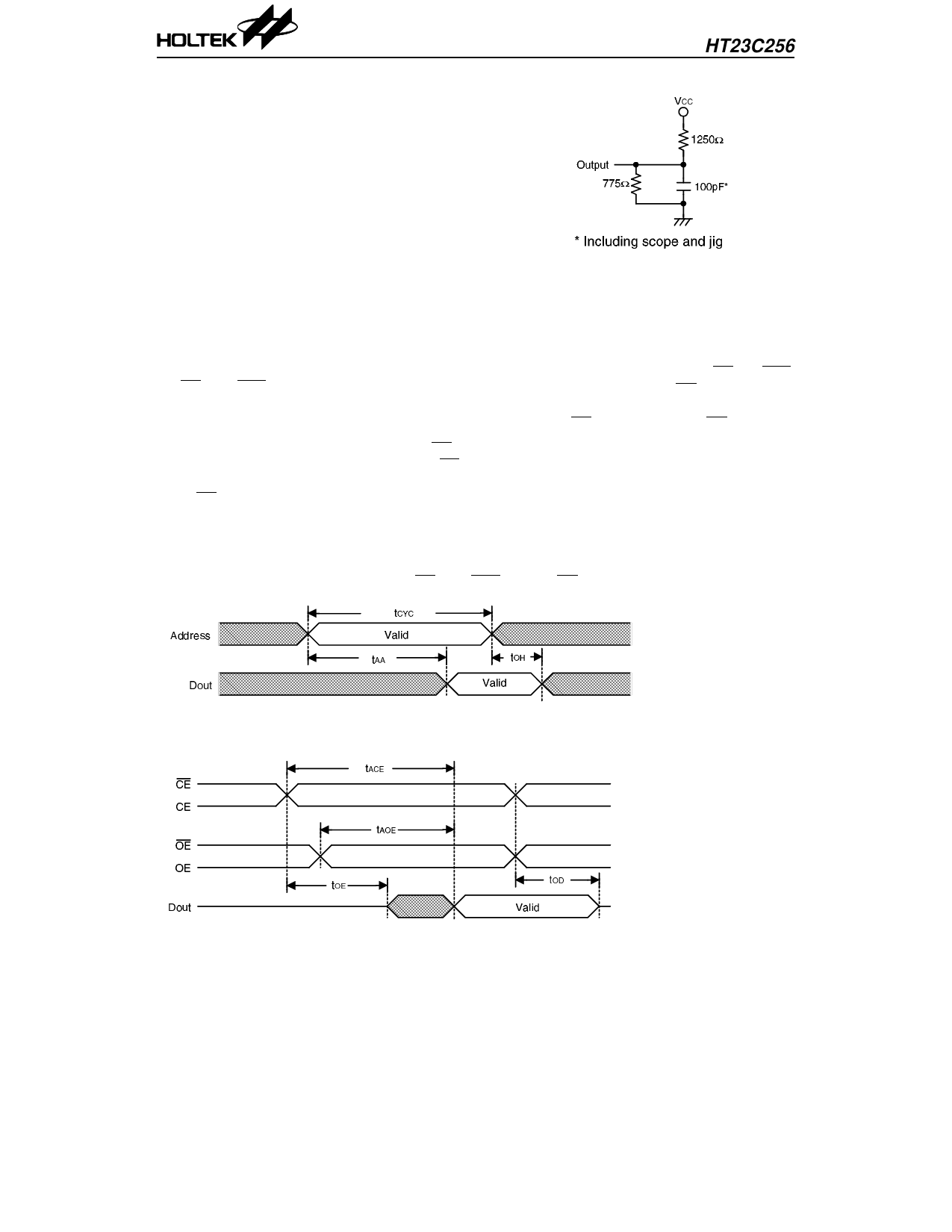
A.C. test conditions
Output load: see figure right
Input rise and fall time: 10ns
Input pulse levels: 0.4V to 2.4V
Input and output timing reference levels:
0.8V and 2.0V (VCC=5V), 1.5V (VCC=3V)
HT23C256
Output load circuit
Functional Description
The HT23C256 has two modes, namely data
read mode and standby mode, controlled by
CE/CE/OE1/OE1 and OE/OE/NC inputs.
• Standby mode
The HT23C256 has lower current consumption,
controlled by the chip enable input (CE/CE).
When a low/high level is applied to the CE/CE
input regardless of the output enable
(OE/OE/NC) states the chip will enter the
standby mode.
• Data read mode
When both the chip enable (CE/CE/OE/OE1)
and the output enable (OE/OE/NC) are active,
the chip is in data read mode. Otherwise,
active CE/CE and inactive OE/OE/NC result
in deselect mode. The output will remain in
Hi-Z state.
Timing Diagrams
• Propagation delay due to address (CE/CE/OE1/OE1 and OE/OE are active)
• Propagation delay due to chip enable and output enable (address valid)
5
24th Aug ’98
Share Link: 