AS6UA25616-BI жҹҘзңӢж•ёж“ҡиЎЁпјҲPDFпјү - Alliance Semiconductor
йӣ¶д»¶зј–еҸ·
дә§е“ҒжҸҸиҝ° (еҠҹиғҪ)
з”ҹдә§еҺӮ家
AS6UA25616-BI
Alliance Semiconductor

AS6UA25616-BI Datasheet PDF : 9 Pages
| |||
AS6UA25616
В®
Functional description
The AS6UA25616 is a low-power CMOS 4,194,304-bit Static Random Access Memory (SRAM) device organized as 262,144 words x 16
bits. It is designed for memory applications where slow data access, low power, and simple interfacing are desired.
Equal address access and cycle times (tAA, tRC, tWC) of 55/70 ns are ideal for low-power applications. Active high and low chip enables
(CS) permit easy memory expansion with multiple-bank memory systems.
When CS is high, or UB and LB are high, the device enters standby mode: the AS6UA25616 is guaranteed not to exceed 72 ВөW power
consumption at 3.6V and 55 ns; 41ВөW at 2.7V and 70 ns. The device also returns data when VCC is reduced to 1.5V for even lower power
consumption.
A write cycle is accomplished by asserting write enable (WE) and chip enable (CS) low, and UB and/or LB low. Data on the input pins
I/O1вҖ“O16 is written on the rising edge of WE (write cycle 1) or CS (write cycle 2).To avoid bus contention, external devices should drive
I/O pins only after outputs have been disabled with output enable (OE) or write enable (WE).
A read cycle is accomplished by asserting output enable (OE), chip enable (CS), UB and LB low, with write enable (WE) high. The chip
drives I/O pins with the data word referenced by the input address. When either chip enable or output enable is inactive, or write enable is
active, or (UB) and (LB), output drivers stay in high-impedance mode.
These devices provide multiple center power and ground pins, and separate byte enable controls, allowing individual bytes to bewritten
and read. LB controls the lower bits, I/O1вҖ“I/O8, and UB controls the higher bits, I/O9вҖ“I/O16.
All chip inputs and outputs are CMOS-compatible, and operation is from a single 2.3V to 3.6V supply. Device is available in the JEDEC
standard 400-mm, TSOP II, and 48-ball FBGA packages.
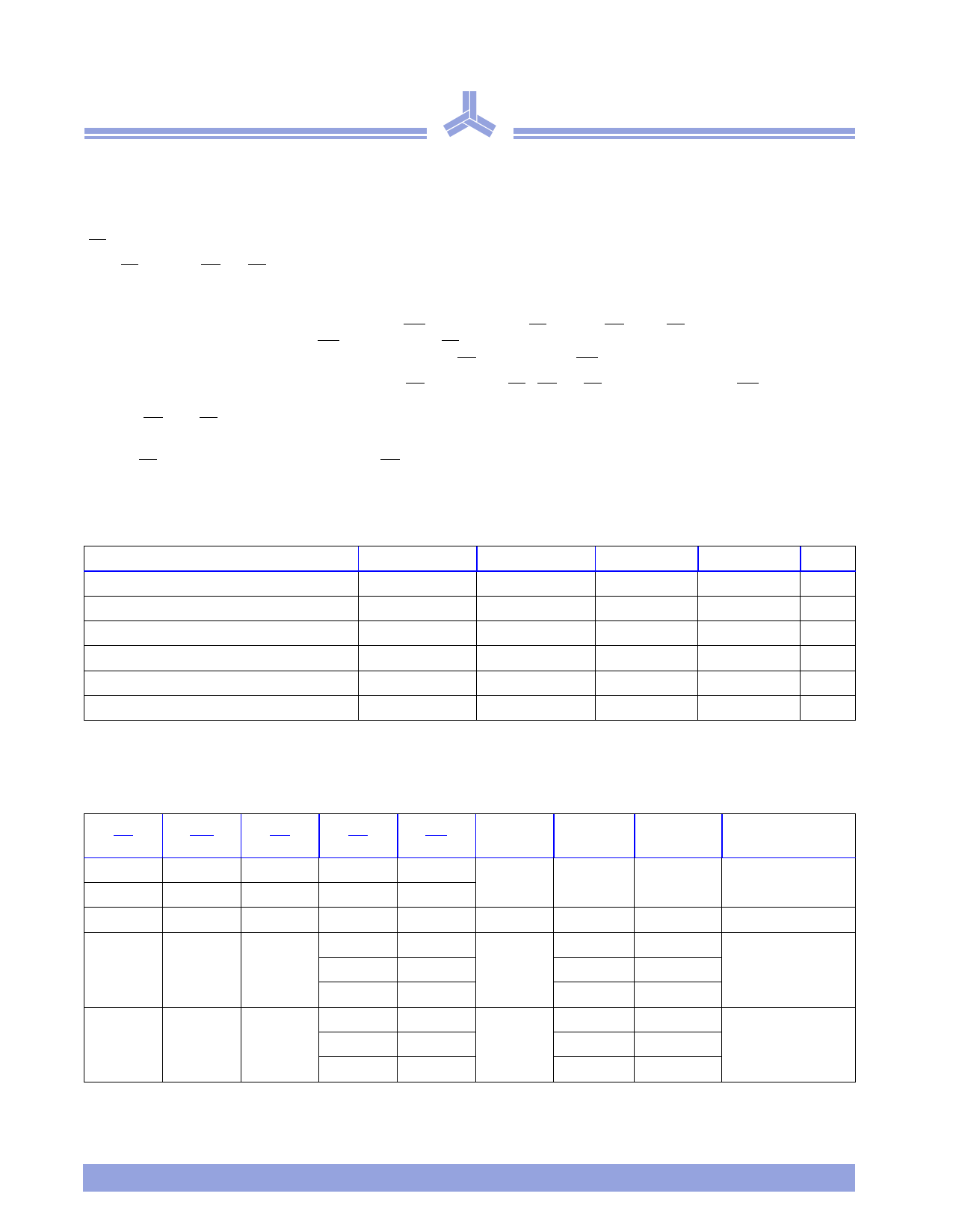
Absolute maximum ratings
Parameter
Device
Symbol
Min
Max
Unit
Voltage on VCC relative to VSS
VtIN
вҖ“0.5
VCC + 0.5
V
Voltage on any I/O pin relative to GND
VtI/O
вҖ“0.5
V
Power dissipation
Storage temperature (plastic)
Temperature with VCC applied
PD
Tstg
Tbias
вҖ“
1.0
W
вҖ“65
+150
oC
вҖ“55
+125
oC
DC output current (low)
IOUT
вҖ“
20
mA
Note: Stresses greater than those listed under Absolute Maximum Ratings may cause permanent damage to the device. This is a stress rating only and
functional operation of the device at these or any other conditions outside those indicated in the operational sections of this specification is not implied.
Exposure to absolute maximum rating conditions for extended periods may affect reliability.
Truth table
Supply
CS
WE
OE
LB
UB
Current I/O1вҖ“I/O8 I/O9вҖ“I/O16
Mode
H
X
X
X
X
L
X
X
H
H
ISB
High Z High Z
Standby (ISB)
L
H
H
X
X
ICC
High Z
High Z Output disable (ICC)
L
H
DOUT
High Z
L
H
L
H
L
ICC
High Z
DOUT
Read (ICC)
L
L
DOUT
DOUT
L
H
DIN
High Z
L
L
X
H
L
ICC
High Z
DIN
Write (ICC)
L
L
DIN
DIN
Key: X = DonвҖҷt care, L = Low, H = High.
2
ALLIANCE SEMICONDUCTOR
10/6/00
Share Link: