VSC8162 查看數據表(PDF) - Vitesse Semiconductor
零件编号
产品描述 (功能)
生产厂家
VSC8162 Datasheet PDF : 20 Pages
| |||
VITESSE
SEMICONDUCTOR CORPORATION
2.488 Gbit/sec SONET/SDH
1:16 Demux with Clock Recovery
Advance Product Information
VSC8162
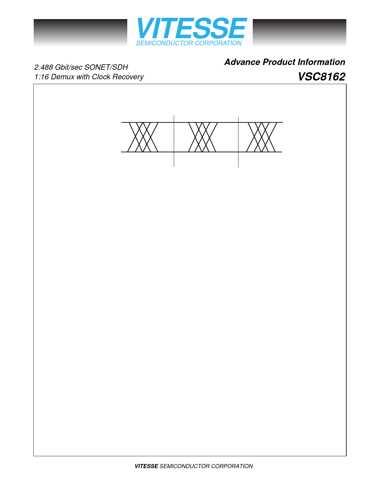
Figure 1: Retiming Offset
DI
Sampling point at the
center of the eye
PH_ADJ[4:0] = 00000
Sampling point
delayed ~50ps from
the center of the eye
PH_ADJ[4:0] = 00100
1:16 Demultiplexer
The demultiplexer inside of the VSC8162 consists of a 1:16 demultiplexer and timing circuitry which gen-
erates a divide-by-16 clock from the high speed clock input. The demultiplexer accepts a serial data stream
input (DI+/DI-) at 2.488 Gb/s and deserializes it into 16 parallel differential outputs (D0..D15). The timing
parameters of the parallel data outputs (D0..D15) are specified with respect to the falling edge of CLK16, so
that CLK16 can be used to clock the destination of D0..D15.
The parity output of the demultiplexer is the XOR of all 16 parallel outputs. The DINVERT input is an ECL
input (see Table 6) which can be used to invert the sense of the data through the demultiplexer. If DINVERT is
left floating, it defaults to the low state, which is the state that corresponds to normal operation (no data inver-
sion).
FILTI, FILTO Pins
The FILTI and FILTO pins are used to provide additional capacitance to the loop filter of the VCO. To opti-
mize the VCO’s performance, it is recommended that 0.1µF, size 0805 capacitors are connected between the
FILTI+ and FILTI- pins, as well as the FILTO+ and FILTO- pins.
Supplies
The VSC8161 is designed to operate with VEE = -5.2V, VTT = -2.0V and VCC = GND (0.0V). However,
the part can be operated in an all positive supply environment, or a mixed positive and negative supply environ-
ment.
To operate in an all positive supply environment, each of the supply voltages must be shifted up by 5.2V
such that VEE will now be GND, VTT = +3.2V and VCC = +5.2V. To operate in a mixed positive and negative
supply environment, each of the supply voltages must be shifted up by 2.0V such that VTT will now be GND,
VEE = -3.2V and VCC = +2.0V.
Bear in mind that termination voltages must be adjusted to reflect any shift in supply voltages.
Page 4
© VITESSE SEMICONDUCTOR CORPORATION
741 Calle Plano, Camarillo, CA 93012 • 805/388-3700 • FAX: 805/987-5896
G52209-0, Rev. 2.0
9/14/98
Share Link: 