2SJ340 查看數據表(PDF) - SANYO -> Panasonic
零件编号
产品描述 (功能)
生产厂家
2SJ340 Datasheet PDF : 4 Pages
| |||
2SJ340
Specifications
Absolute Maximum Ratings at Ta = 25˚C
Parameter
Drain-to-Source Voltage
Gate-to-Source Voltage
Drain Current (DC)
Drain Current (Pulse)
Symbol
VDSS
VGSS
ID
IDP
Allowable Power Dissipation
PD
Channel Temperature
Tch
Storage Temperature
Tstg
Electrical Characteristics at Ta = 25˚C
Conditions
PW≤10µs, duty cycle≤1%
Tc=25˚C
Parameter
Drain-to-Source Breakdown Voltage
Gate-to-Source Breakdown Voltage
Zero-Gate Voltage Drain Current
Gate-to-Source Leakage Current
Cutoff Voltage
Forward Transfer Admittance
Static Drain-to-Source On-State Resistance
Input Capacitance
Output Capacitance
Reverse Transfer Capacitance
Turn-ON Delay Time
Rise Time
Turn-OFF Delay Time
Fall Time
Diode Forward Voltage
Marking:J304
Symbol
Conditions
V(BR)DSS
V(BR)GSS
IDSS
IGSS
VGS(off)
| yfs |
RDS(on)1
RDS(on)2
Ciss
Coss
Crss
td(on)
tr
td(off)
tf
VSD
ID=–1mA, VGS=0
IG=±100µA, VDS=0
VDS=–60V, VGS=0
VGS=±16V, VDS=0
VDS=–10V, ID=–1mA
VDS=–10V, ID=–15A
ID=–15A, VGS=–10V
ID=–15A, VGS=–4V
VDS=–20V, f=1MHz
VDS=–20V, f=1MHz
VDS=–20V, f=1MHz
See specified Test Circuit
See specified Test Circuit
See specified Test Circuit
See specified Test Circuit
IS=–30A, VGS=0
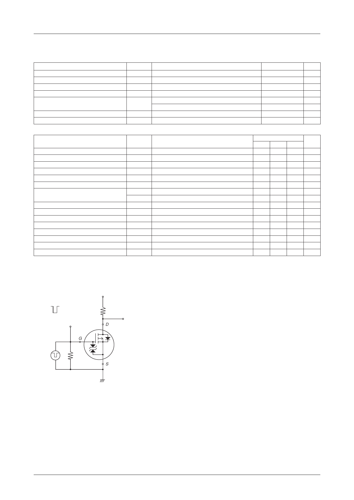
Switching Time Test Circuit
Vin
0V
--10V
PW=10µs
D.C.≤1%
P.G
Vin
G
50Ω
VDD=--30V
ID=--15A
RL=2Ω
D
VOUT
2SJ340
S
Ratings
Unit
–60 V
±20 V
–30 A
–120 A
1.65 W
70 W
150 ˚C
–55 to +150 ˚C
Ratings
Unit
min
typ
max
–60
V
±20
V
–100 µA
±10 µA
–1.0
–2.0 V
15
25
S
30
40 mΩ
40
55 mΩ
3800
pF
1200
pF
300
pF
30
ns
150
ns
450
ns
220
ns
–1.0 –1.5 V
No.6420–2/4
Share Link: 