2SJ509 查看數據表(PDF) - Toshiba
零件编号
产品描述 (功能)
生产厂家
2SJ509 Datasheet PDF : 3 Pages
| |||
2SJ509
TOSHIBA Field Effect Transistor Silicon P Channel MOS Type (L2−π−MOSV)
2SJ509
Chopper Regulator, DC−DC Converter and Motor Drive
Applications
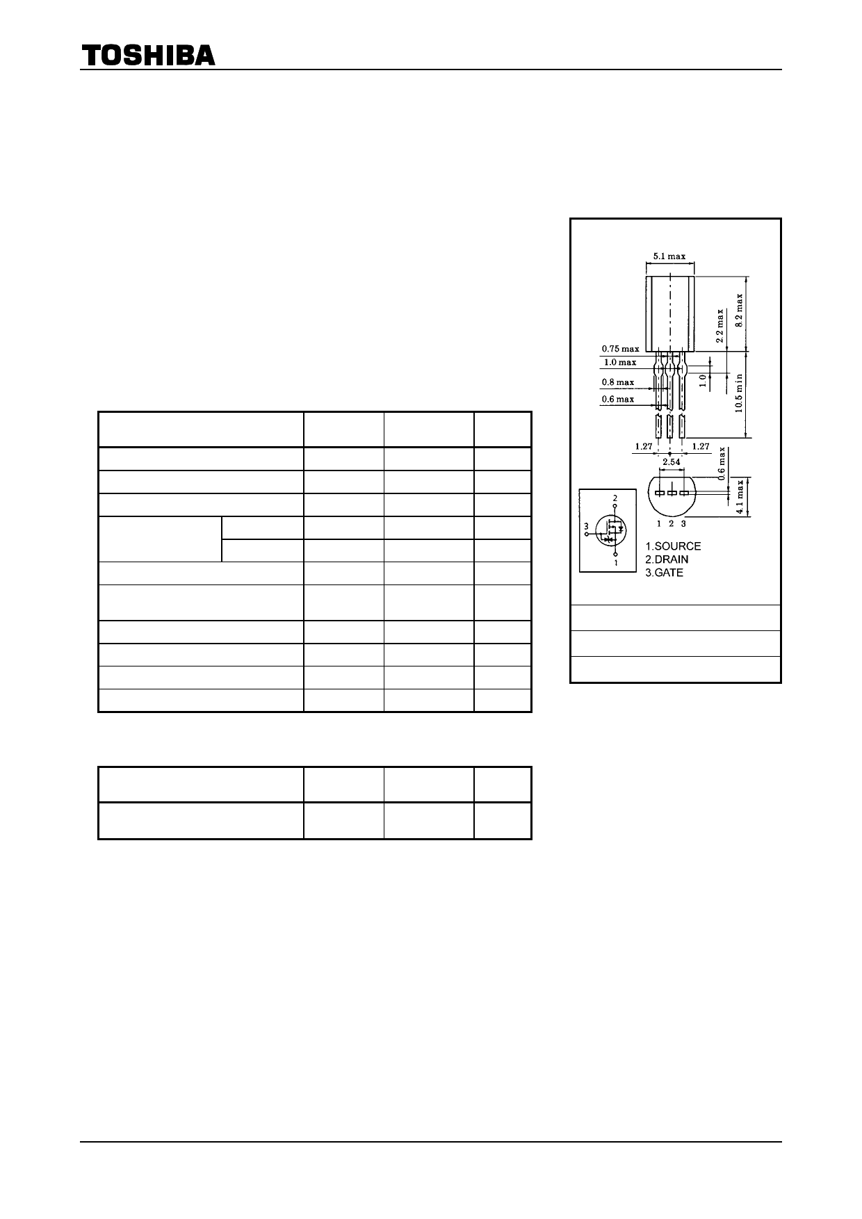
Unit: mm
l 4 V gate drive
l Low drain−source ON resistance
: RDS (ON) = 1.35 Ω (typ.)
l High forward transfer admittance : |Yfs| = 0.7 S (typ.)
l Low leakage current : IDSS = −100 µA (max) (VDS = −100 V)
l Enhancement−mode : Vth = −0.8~−2.0 V (VDS = −10 V, ID = −1 mA)
Maximum Ratings (Ta = 25°C)
Characteristics
Symbol
Rating
Unit
Drain−source voltage
Drain−gate voltage (RGS = 20 kΩ)
Gate−source voltage
Drain current
DC (Note 1)
Pulse (Note 1)
Drain power dissipation (Ta = 25°C)
Single pulse avalanche energy
(Note 2)
Avalanche current
Repetitive avalanche energy (Note 3)
Channel temperature
Storage temperature range
VDSS
VDGR
VGSS
ID
IDP
PD
EAS
IAR
EAR
Tch
Tstg
−100
V
−100
V
±20
V
−1
A
−3
A
0.9
W
136.5
mJ
−1
A
0.09
mJ
150
°C
−55~150
°C
JEDEC
TO-92MOD
JEITA
―
TOSHIBA
2-5J1C
Weight: 0.36 g (typ.)
Thermal Characteristics
Characteristics
Symbol
Max
Unit
Thermal resistance, channel to
ambient
Rth (ch−a)
138
°C / W
Note 1: Please use devices on condition that the channel temperature is below 150°C.
Note 2: VDD = −50 V, Tch = 25°C (initial), L = 168 mH, RG = 25 Ω, IAR = −1 A
Note 3: Repetitive rating; Pulse width limited by maximum channel temperature.
This transistor is an electrostatic sensitive device.
Please handle with caution.
1
2002-01-25
Share Link: 