2SJ526-E 查看數據表(PDF) - Renesas Electronics
零件编号
产品描述 (功能)
生产厂家
2SJ526-E Datasheet PDF : 10 Pages
| |||
2SJ526
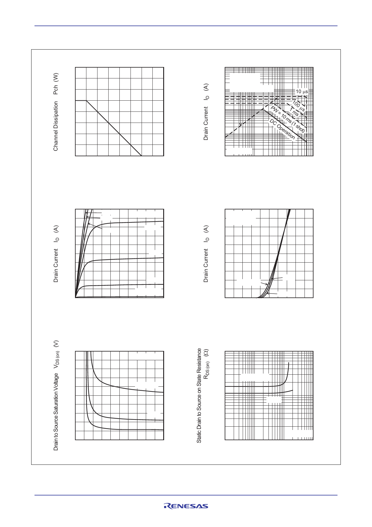
Main Characteristics
Power vs. Temperature Derating
40
30
20
10
0
0
50
100
150
200
Case Temperature Tc (°C)
Typical Output Characteristics
–10
–10 V
Pulse Test
–5 V
–8
–4 V
–3.5 V
–6
–3 V
–4
–2
–2.5 V
VGS = –2 V
0
0
–2 –4 –6 –8 –10
Drain to Source Voltage VDS (V)
Drain to Source Saturation Voltage vs.
Gate to Source Voltage
–1.0
Pulse Test
–0.8
–0.6
ID = –5 A
–0.4
–2 A
–0.2
–1 A
0
0
–4
–8 –12 –16 –20
Gate to Source Voltage VGS (V)
Rev.6.00 Jun 05, 2006 page 3 of 7
Maximum Safe Operation Area
–1000
–300
–100
Operation in
this area is
limited by RDS (on)
10 µs
–30
–10
–3
–1
DPCWO=p1e0ramtis1o(n1m10ss0hoµts)
–0.3
Ta = 25°C
–0.1
–0.1 –0.3 –1 –3 –10 –30 –100
Drain to Source Voltage VDS (V)
Typical Transfer Characteristics
–10
VDS = –10 V
Pulse Test
–8
–6
–4
–2
Tc = 75°C
25°C
–25°C
0
0
–1 –2 –3 –4 –5
Gate to Source Voltage VGS (V)
Static Drain to Source on State Resistance
vs. Drain Current
1
0.5
VGS = –4 V
0.2
0.1
–10 V
0.05
0.02
Pulse Test
0.01
–0.1 –0.3 –1 –3 –10 –30 –100
Drain Current ID (A)
Share Link: 